Hdi layer pcb
Understanding The Benefits Of HDI Layer PCB In Modern Electronics
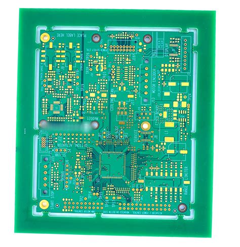
High-Density Interconnect (HDI) layer printed circuit boards (PCBs) have become a cornerstone in the advancement of modern electronics, offering a multitude of benefits that cater to the ever-evolving demands of technology. As electronic devices continue to shrink in size while increasing in functionality, the need for more efficient and compact circuit board designs has become paramount. HDI layer PCBs address this need by providing a solution that enhances performance, reliability, and design flexibility.
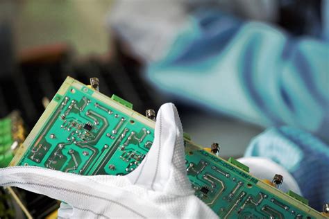
One of the primary advantages of HDI layer PCBs is their ability to accommodate a higher density of components on a smaller board area.
This is achieved through the use of microvias, blind vias, and buried vias, which allow for more intricate routing of electrical connections. Consequently, designers can place components closer together, reducing the overall size of the PCB. This miniaturization is particularly beneficial in the development of portable electronic devices such as smartphones, tablets, and wearable technology, where space is at a premium.
Moreover, HDI layer PCBs contribute to improved electrical performance.
The shorter distances between components result in reduced signal loss and lower electromagnetic interference, which are critical factors in high-speed and high-frequency applications. This enhancement in signal integrity ensures that devices operate more efficiently and with greater reliability, which is essential in sectors such as telecommunications, aerospace, and medical devices, where precision and dependability are non-negotiable.
In addition to performance improvements, HDI layer PCBs offer significant design flexibility.
The ability to incorporate multiple layers and complex interconnections allows engineers to create more sophisticated and innovative designs. This flexibility is crucial in the development of cutting-edge technologies, enabling the integration of advanced features and functionalities that were previously unattainable with traditional PCB designs. As a result, manufacturers can push the boundaries of what is possible, leading to the creation of more powerful and versatile electronic products.
Furthermore, the use of HDI layer PCBs can lead to cost savings in the long run.
Although the initial manufacturing costs may be higher due to the complexity of the design and fabrication processes, the benefits of reduced material usage, smaller form factors, and enhanced performance can offset these expenses. Additionally, the increased reliability and durability of HDI layer PCBs can result in lower maintenance and repair costs over the product’s lifecycle, providing further economic advantages.
The environmental impact of HDI layer PCBs is also worth noting.
By enabling the production of smaller and more efficient devices, these PCBs contribute to the reduction of electronic waste. Smaller devices require fewer raw materials and consume less energy, aligning with the growing emphasis on sustainability in the electronics industry. As companies strive to meet environmental regulations and consumer expectations for eco-friendly products, the adoption of HDI layer PCBs can play a pivotal role in achieving these goals.
In conclusion, HDI layer PCBs represent a significant advancement in the field of electronics, offering a range of benefits that address the challenges of modern technology. Their ability to support higher component densities, improve electrical performance, provide design flexibility, and offer cost and environmental advantages makes them an indispensable component in the development of next-generation electronic devices. As the demand for more compact, efficient, and sustainable technology continues to grow, the role of HDI layer PCBs in shaping the future of electronics is set to become increasingly prominent.
Design Challenges And Solutions For HDI Layer PCB
High-Density Interconnect (HDI) layer PCBs have become a cornerstone in the advancement of modern electronics, offering significant benefits in terms of size reduction, performance enhancement, and increased functionality. However, designing HDI layer PCBs presents a unique set of challenges that require innovative solutions to ensure optimal performance and reliability. As the demand for more compact and efficient electronic devices continues to grow, understanding these challenges and their corresponding solutions is crucial for engineers and designers in the field.
One of the primary challenges in designing HDI layer PCBs is managing the increased complexity that comes with higher component density.
As devices become smaller, the need to fit more components into a limited space becomes imperative. This often leads to intricate routing and the necessity for multiple layers to accommodate all the connections. To address this, designers employ advanced techniques such as microvias, blind and buried vias, which allow for more efficient use of space by enabling connections between layers without occupying significant surface area. These techniques not only help in managing space but also improve signal integrity by reducing the length of the traces.
Another significant challenge is maintaining signal integrity and minimizing electromagnetic interference (EMI).
As the density of components increases, so does the potential for signal interference, which can degrade the performance of the PCB. To mitigate this, designers must carefully consider the placement of components and the routing of traces. Utilizing ground planes and proper shielding techniques can significantly reduce EMI. Additionally, employing differential signaling and controlled impedance routing can further enhance signal integrity, ensuring that the PCB performs reliably in high-speed applications.
Thermal management is also a critical concern in HDI layer PCB design.
The compact nature of these PCBs means that heat dissipation can become a significant issue, potentially leading to overheating and failure of components. To combat this, designers can incorporate thermal vias and heat sinks to facilitate better heat distribution. Moreover, selecting materials with high thermal conductivity for the PCB substrate can aid in efficient heat management. Advanced simulation tools can also be employed during the design phase to predict thermal behavior and optimize the layout accordingly.
Manufacturability is another aspect that poses challenges in HDI layer PCB design.
The precision required for fabricating these intricate designs demands advanced manufacturing techniques and equipment. Ensuring that the design is manufacturable without compromising on quality or performance is essential. Collaboration with experienced manufacturers during the design phase can provide valuable insights into the limitations and capabilities of current manufacturing technologies, allowing for adjustments that enhance manufacturability.
Finally, cost considerations cannot be overlooked.
The advanced materials and processes required for HDI layer PCBs can lead to increased production costs. Designers must strike a balance between performance requirements and budget constraints. This can be achieved by optimizing the design to use fewer layers where possible, selecting cost-effective materials, and leveraging economies of scale in production.
In conclusion, while HDI layer PCBs offer numerous advantages in the realm of modern electronics, they also present a set of complex design challenges. By employing innovative solutions such as advanced via technology, careful signal integrity management, effective thermal strategies, and close collaboration with manufacturers, designers can overcome these challenges. As technology continues to evolve, the ability to adeptly navigate these challenges will be essential in pushing the boundaries of what is possible in electronic design.
The Role Of HDI Layer PCB In Miniaturization Of Devices
The rapid advancement of technology has ushered in an era where the demand for smaller, more efficient electronic devices is at an all-time high. Central to this trend is the High-Density Interconnect (HDI) layer printed circuit board (PCB), which plays a pivotal role in the miniaturization of electronic devices. As consumer expectations evolve, the need for compact yet powerful gadgets has driven engineers and designers to innovate continuously. HDI layer PCBs have emerged as a cornerstone in this pursuit, offering a solution that balances size reduction with enhanced performance.
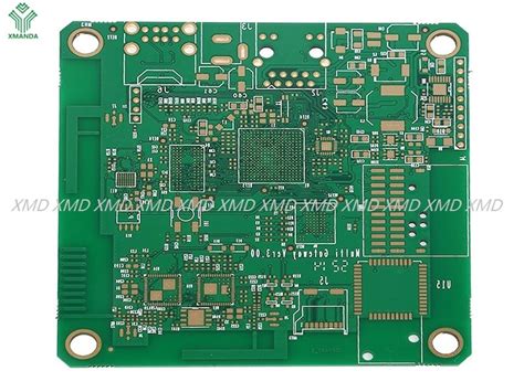
HDI layer PCBs are characterized by their higher wiring density per unit area compared to traditional PCBs.
This is achieved through the use of finer lines and spaces, smaller vias, and capture pads, as well as higher connection pad density. These features allow for more components to be placed on both sides of the PCB, effectively increasing the functionality of the board without expanding its size. Consequently, HDI technology enables the design of smaller, lighter, and more efficient electronic devices, which is crucial in industries such as consumer electronics, telecommunications, and medical devices.
One of the primary advantages of HDI layer PCBs is their ability to support advanced component packaging technologies, such as chip-scale packages (CSPs) and ball grid arrays (BGAs).
These packaging methods are essential for reducing the size of electronic components while maintaining or even enhancing their performance. By facilitating the integration of these advanced packages, HDI PCBs contribute significantly to the miniaturization of devices. Moreover, the use of microvias in HDI PCBs allows for shorter signal paths, which not only improves signal integrity but also reduces signal delay. This is particularly beneficial in high-speed applications where performance is critical.
In addition to supporting advanced packaging technologies, HDI layer PCBs also offer improved thermal management capabilities.
As devices become smaller, managing heat dissipation becomes increasingly challenging. HDI PCBs address this issue by providing better heat distribution, which is essential for maintaining the reliability and longevity of electronic components. This is achieved through the use of materials with superior thermal properties and the strategic placement of vias to facilitate heat transfer.
Furthermore, the adoption of HDI layer PCBs aligns with the growing emphasis on sustainability in electronic design.
By enabling the production of smaller devices, HDI technology contributes to the reduction of material usage and energy consumption during manufacturing. This not only lowers production costs but also minimizes the environmental impact of electronic devices. As a result, HDI PCBs are not only a technical solution but also a step towards more sustainable electronic design practices.
In conclusion, the role of HDI layer PCBs in the miniaturization of devices is both significant and multifaceted.
By offering higher wiring density, supporting advanced packaging technologies, and improving thermal management, HDI PCBs enable the creation of smaller, more efficient electronic devices. As the demand for compact and powerful gadgets continues to grow, the importance of HDI technology in meeting these expectations cannot be overstated. As such, HDI layer PCBs will undoubtedly remain a critical component in the ongoing evolution of electronic device design, driving innovation and sustainability in equal measure.
Comparing HDI Layer PCB With Traditional PCB Technologies
In the ever-evolving landscape of electronics manufacturing, the choice of printed circuit board (PCB) technology plays a crucial role in determining the performance, size, and cost-effectiveness of electronic devices. Among the various PCB technologies available, High-Density Interconnect (HDI) layer PCBs have emerged as a significant advancement over traditional PCB technologies. To understand the advantages and limitations of HDI layer PCBs, it is essential to compare them with their traditional counterparts, focusing on aspects such as design complexity, performance, and manufacturing processes.
HDI layer PCBs are characterized by their ability to accommodate a higher density of components and interconnections within a smaller footprint.
This is achieved through the use of microvias, finer lines and spaces, and multiple layers of interconnections. In contrast, traditional PCBs typically rely on through-hole vias and larger trace widths, which can limit the density of components and the overall miniaturization of the device. Consequently, HDI layer PCBs are particularly advantageous in applications where space is at a premium, such as in smartphones, tablets, and other compact electronic devices.
Moreover, the enhanced design capabilities of HDI layer PCBs contribute to improved electrical performance.
The shorter interconnection paths and reduced parasitic inductance and capacitance in HDI designs lead to faster signal transmission and reduced signal loss. This is particularly beneficial in high-frequency applications, where maintaining signal integrity is paramount. Traditional PCBs, with their longer and more complex routing paths, may struggle to achieve the same level of performance in such demanding environments.
In addition to performance benefits, HDI layer PCBs offer greater design flexibility.
The use of blind and buried vias, along with the ability to stack multiple layers, allows for more complex routing solutions and the integration of additional features without increasing the board size. This flexibility is a significant advantage in the design of multifunctional devices, where multiple components and functionalities need to be integrated into a single compact unit. Traditional PCBs, on the other hand, may require larger board sizes or additional layers to achieve similar functionality, potentially increasing the overall cost and complexity of the device.
However, it is important to acknowledge that the advanced capabilities of HDI layer PCBs come with certain challenges.
The manufacturing processes for HDI PCBs are more complex and require specialized equipment and expertise. This can result in higher production costs compared to traditional PCBs, particularly for low-volume production runs. Additionally, the finer features and smaller vias in HDI designs can pose challenges in terms of reliability and yield, necessitating stringent quality control measures during manufacturing.
Despite these challenges, the benefits of HDI layer PCBs often outweigh the drawbacks, especially in applications where size, performance, and functionality are critical considerations. As electronic devices continue to shrink in size while increasing in complexity, the demand for HDI layer PCBs is expected to grow, driving further advancements in manufacturing technologies and design methodologies.
In conclusion, while traditional PCB technologies continue to serve a wide range of applications effectively, HDI layer PCBs offer distinct advantages in terms of miniaturization, performance, and design flexibility. As the electronics industry continues to push the boundaries of what is possible, the role of HDI layer PCBs is likely to become increasingly prominent, shaping the future of electronic device design and manufacturing.