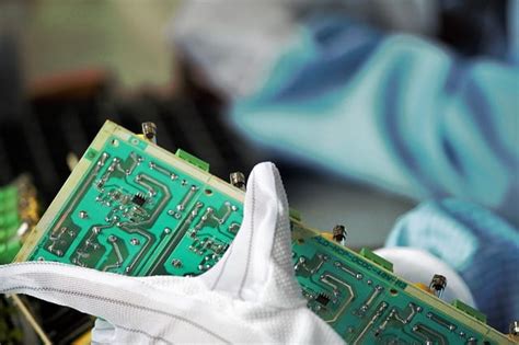
Hdi multilayer pcb
Advantages Of HDI Multilayer PCB In Modern Electronics
High-Density Interconnect (HDI) multilayer printed circuit boards (PCBs) have become a cornerstone in the advancement of modern electronics, offering a multitude of advantages that cater to the ever-evolving demands of technology. As electronic devices continue to shrink in size while increasing in functionality, the need for more efficient and compact circuit board designs has become paramount. HDI multilayer PCBs address these needs by providing a sophisticated solution that enhances performance, reliability, and design flexibility.
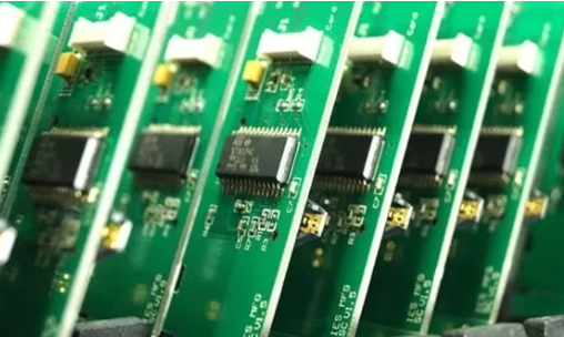
One of the primary advantages of HDI multilayer PCBs is their ability to support higher component density.
By utilizing microvias, blind vias, and buried vias, these PCBs can accommodate more components on a single board without increasing its size. This capability is crucial in the development of compact devices such as smartphones, tablets, and wearable technology, where space is at a premium. The increased component density not only allows for more complex circuitry but also contributes to the miniaturization of electronic devices, a trend that is increasingly prevalent in consumer electronics.
In addition to supporting higher component density, HDI multilayer PCBs offer improved electrical performance.
The shorter interconnect paths made possible by the use of microvias reduce signal loss and improve signal integrity. This is particularly beneficial in high-frequency applications where maintaining signal quality is critical. Furthermore, the reduced parasitic capacitance and inductance in HDI designs contribute to faster signal transmission, which is essential for high-speed data processing and communication applications. As a result, devices that incorporate HDI multilayer PCBs can achieve superior performance and efficiency.
Another significant advantage of HDI multilayer PCBs is their enhanced thermal management capabilities.
The increased number of layers and the use of advanced materials in HDI designs facilitate better heat dissipation, which is vital for maintaining the reliability and longevity of electronic components. Effective thermal management is especially important in high-power applications, where excessive heat can lead to component failure and reduced performance. By efficiently managing heat, HDI multilayer PCBs help ensure the stability and durability of electronic devices.
Moreover, HDI multilayer PCBs offer greater design flexibility, allowing engineers to create more innovative and complex designs.
The ability to incorporate multiple layers and advanced interconnect techniques enables the integration of diverse functionalities within a single board. This flexibility is particularly advantageous in the development of multifunctional devices that require the seamless integration of various components and systems. Consequently, HDI multilayer PCBs empower designers to push the boundaries of what is possible in electronic design, leading to the creation of cutting-edge products that meet the demands of modern consumers.
In conclusion, the advantages of HDI multilayer PCBs in modern electronics are manifold, encompassing higher component density, improved electrical performance, enhanced thermal management, and greater design flexibility. These benefits make HDI multilayer PCBs an indispensable component in the development of advanced electronic devices. As technology continues to evolve, the role of HDI multilayer PCBs in enabling innovation and meeting the challenges of modern electronics will undoubtedly remain significant. By leveraging the capabilities of HDI technology, manufacturers can continue to produce smaller, faster, and more efficient devices that cater to the needs of an increasingly connected world.
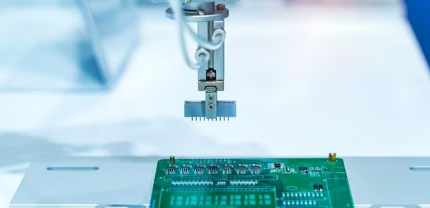
Design Considerations For HDI Multilayer PCB Manufacturing
In the realm of modern electronics, High-Density Interconnect (HDI) multilayer printed circuit boards (PCBs) have emerged as a pivotal technology, enabling the miniaturization and enhanced performance of electronic devices. As the demand for compact and efficient electronic products continues to rise, understanding the design considerations for HDI multilayer PCB manufacturing becomes increasingly crucial. These considerations not only influence the functionality and reliability of the final product but also impact the overall manufacturing process.
To begin with, one of the primary design considerations for HDI multilayer PCBs is the selection of materials.
The choice of substrate material is critical, as it affects the board’s thermal and electrical performance. Materials with high glass transition temperatures (Tg) and low coefficients of thermal expansion (CTE) are often preferred, as they provide better stability under thermal stress. Additionally, the dielectric constant and loss tangent of the material must be considered to ensure signal integrity, especially in high-frequency applications.
Transitioning to the aspect of layer stack-up, it is essential to carefully plan the arrangement of layers in an HDI multilayer PCB.
The stack-up design influences the board’s impedance control, signal integrity, and thermal management. A well-optimized stack-up can minimize electromagnetic interference (EMI) and crosstalk, which are critical for maintaining signal quality. Furthermore, the use of microvias, blind vias, and buried vias in HDI designs allows for more efficient routing and interconnection of layers, thereby reducing the board’s overall size and weight.
Another significant consideration is the aspect ratio of vias, which is the ratio of the hole depth to its diameter.
In HDI multilayer PCBs, maintaining a low aspect ratio is vital to ensure reliable via plating and to prevent issues such as voids or incomplete plating. This is particularly important for microvias, which are smaller in diameter compared to traditional vias. The use of laser drilling technology has become prevalent in HDI manufacturing, as it allows for precise and consistent microvia formation.
Moreover, signal integrity is a paramount concern in HDI multilayer PCB design.
As electronic devices operate at higher speeds, the risk of signal degradation increases. To mitigate this, designers must consider factors such as trace width, spacing, and the use of differential pairs. Impedance matching is also crucial to prevent signal reflections and losses. Advanced simulation tools can aid in predicting and optimizing signal behavior, ensuring that the final design meets the desired performance criteria.
Thermal management is another critical aspect that cannot be overlooked.
As electronic components become more densely packed, effective heat dissipation becomes challenging. Incorporating thermal vias, heat sinks, and thermal pads into the design can help manage heat distribution and prevent overheating. Additionally, selecting materials with high thermal conductivity can further enhance the board’s ability to dissipate heat.
In conclusion, the design considerations for HDI multilayer PCB manufacturing are multifaceted and require a comprehensive understanding of material properties, layer stack-up, via technology, signal integrity, and thermal management. By carefully addressing these factors, designers can create HDI multilayer PCBs that meet the demands of modern electronic applications, ensuring reliability, performance, and manufacturability. As technology continues to evolve, staying abreast of advancements in HDI design and manufacturing techniques will be essential for producing cutting-edge electronic products.
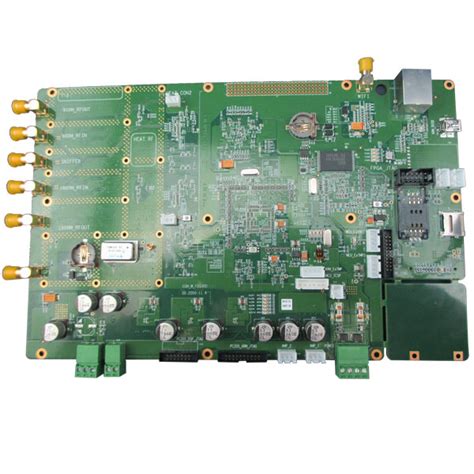
Comparing HDI Multilayer PCB To Traditional PCB Technologies
In the realm of printed circuit board (PCB) technologies, the evolution from traditional PCBs to High-Density Interconnect (HDI) multilayer PCBs marks a significant advancement in electronic design and manufacturing. As electronic devices become increasingly compact and complex, the demand for more efficient and capable PCBs has surged. HDI multilayer PCBs have emerged as a solution to meet these demands, offering distinct advantages over traditional PCB technologies.
To begin with, HDI multilayer PCBs are characterized by their higher wiring density per unit area compared to traditional PCBs.
This is achieved through the use of microvias, blind vias, and buried vias, which allow for more interconnections in a smaller space. Consequently, HDI technology enables the design of smaller, lighter, and more powerful electronic devices. In contrast, traditional PCBs, which typically use through-hole vias, are limited in their ability to support high-density designs. This limitation often results in larger and bulkier boards, which can be a significant drawback in applications where space is at a premium.
Moreover, the enhanced electrical performance of HDI multilayer PCBs is another critical factor that sets them apart from traditional PCBs.
The shorter signal paths in HDI designs reduce signal loss and improve signal integrity, which is crucial for high-speed and high-frequency applications. Traditional PCBs, with their longer and more complex signal paths, may struggle to maintain signal integrity in such demanding applications. This makes HDI technology particularly advantageous in industries such as telecommunications, aerospace, and consumer electronics, where performance and reliability are paramount.
In addition to improved electrical performance, HDI multilayer PCBs offer greater design flexibility.
The ability to incorporate more layers and finer lines allows designers to create more intricate and sophisticated circuits. This flexibility is essential for integrating advanced features and functionalities into modern electronic devices. Traditional PCBs, on the other hand, are often constrained by their limited layer count and larger trace widths, which can restrict design possibilities and innovation.
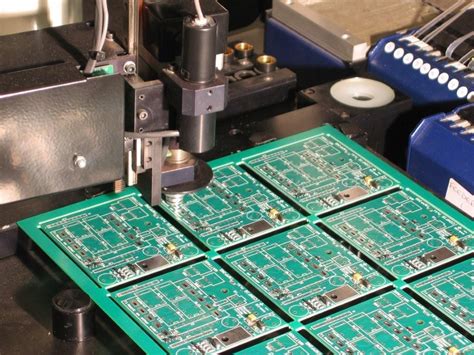
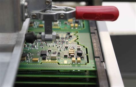
Furthermore, the manufacturing process for HDI multilayer PCBs, while more complex, offers several benefits over traditional PCB manufacturing.
The use of advanced materials and techniques, such as laser drilling and sequential lamination, enables the production of highly reliable and durable boards. These processes also contribute to the overall miniaturization of electronic components, aligning with the industry’s trend towards smaller and more efficient devices. Although traditional PCBs are generally easier and less expensive to produce, they may not offer the same level of performance and reliability required for cutting-edge applications.
Despite the numerous advantages of HDI multilayer PCBs, it is important to acknowledge that they may not be the ideal solution for every application.
The increased complexity and cost associated with HDI technology can be prohibitive for simpler or cost-sensitive projects. In such cases, traditional PCBs may still be the preferred choice, offering a more economical and straightforward solution.
In conclusion, the comparison between HDI multilayer PCBs and traditional PCB technologies highlights the significant advancements that HDI technology brings to the table. With their higher density, improved electrical performance, and greater design flexibility, HDI multilayer PCBs are well-suited for the demands of modern electronic devices. However, the choice between HDI and traditional PCBs ultimately depends on the specific requirements and constraints of each project, underscoring the importance of careful consideration in the design and manufacturing process.
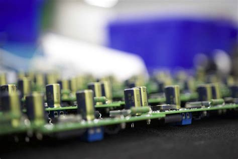
Future Trends In HDI Multilayer PCB Development
The development of High-Density Interconnect (HDI) multilayer printed circuit boards (PCBs) has been a cornerstone in advancing modern electronics, and as we look to the future, several trends are poised to further revolutionize this field. As electronic devices continue to shrink in size while increasing in functionality, the demand for more compact, efficient, and reliable PCBs is growing. HDI technology, with its ability to support higher wiring density and finer lines and spaces, is at the forefront of meeting these demands.
One of the most significant trends in HDI multilayer PCB development is the push towards even greater miniaturization.
As consumer electronics, such as smartphones and wearable devices, become more compact, the need for smaller components that do not compromise performance is critical. HDI PCBs, with their microvias and thin lines, allow for more components to be packed into a smaller area, thus supporting the trend towards miniaturization. This trend is further driven by the Internet of Things (IoT), where devices require efficient and compact PCBs to function effectively in a networked environment.
In addition to miniaturization, the integration of advanced materials is another trend shaping the future of HDI multilayer PCBs.
The use of materials such as liquid crystal polymer (LCP) and polytetrafluoroethylene (PTFE) is becoming more prevalent. These materials offer superior electrical properties, such as lower dielectric constants and reduced signal loss, which are essential for high-frequency applications. As the demand for faster data transmission and higher bandwidth continues to rise, the adoption of these advanced materials in HDI PCBs is expected to increase.
Moreover, the evolution of manufacturing techniques is playing a crucial role in the development of HDI multilayer PCBs.
Techniques such as laser drilling and advanced lamination processes are enabling the production of PCBs with even finer features and more layers. These advancements not only improve the performance and reliability of the PCBs but also reduce production costs, making HDI technology more accessible to a broader range of applications. As these manufacturing techniques continue to evolve, they will likely lead to further innovations in HDI PCB design and functionality.
Furthermore, the growing emphasis on sustainability and environmental responsibility is influencing the development of HDI multilayer PCBs.
Manufacturers are increasingly focusing on reducing waste and energy consumption during the production process. This includes the use of eco-friendly materials and the implementation of recycling programs for PCB components. As environmental regulations become more stringent, the industry is expected to continue its shift towards more sustainable practices, which will impact the design and production of HDI PCBs.
Finally, the integration of artificial intelligence (AI) and machine learning in the design and testing of HDI multilayer PCBs is an emerging trend that holds great promise.
These technologies can optimize PCB layouts, predict potential failures, and enhance the overall design process, leading to more efficient and reliable products. As AI and machine learning technologies advance, their application in HDI PCB development is likely to expand, offering new possibilities for innovation.
In conclusion, the future of HDI multilayer PCB development is marked by trends such as miniaturization, the use of advanced materials, evolving manufacturing techniques, sustainability, and the integration of AI. These trends are not only shaping the current landscape but also setting the stage for future advancements in the field, ensuring that HDI technology remains at the forefront of electronic innovation.