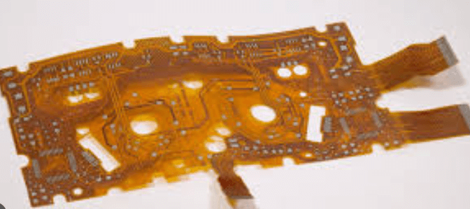
Hdi pcb application
Enhancing Signal Integrity in HDI PCB Designs
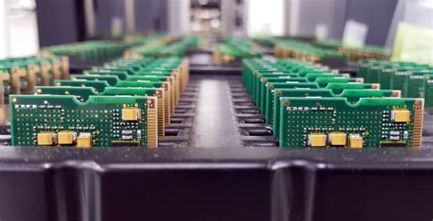
High-Density Interconnect (HDI) Printed Circuit Boards (PCBs) have become a cornerstone in modern electronics, primarily due to their ability to enhance signal integrity. As electronic devices continue to shrink in size while increasing in functionality, the demand for HDI PCBs has surged. These advanced circuit boards are designed to accommodate more components in a smaller area, thereby improving performance and reliability.
One of the most significant advantages of HDI PCBs is their ability to maintain signal integrity
which is crucial for the efficient operation of high-speed electronic devices.
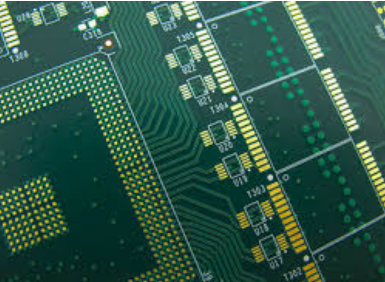
Signal integrity refers to the quality and reliability of electrical signals as they travel through a PCB. In high-speed circuits, maintaining signal integrity is paramount to ensure that data is transmitted accurately and without distortion. HDI PCBs achieve this through several design features that mitigate issues such as signal loss, crosstalk, and electromagnetic interference (EMI). For instance, the use of microvias, which are smaller than traditional vias, allows for shorter signal paths. This reduction in path length minimizes signal loss and improves overall performance.
Moreover, HDI PCBs often incorporate multiple layers, which provide additional routing options and help in separating high-speed signals from power and ground planes.
This separation is essential in reducing crosstalk, a phenomenon where signals in adjacent traces interfere with each other. By strategically placing these layers, designers can ensure that high-speed signals are isolated, thereby preserving their integrity. Additionally, the use of advanced materials with low dielectric constants and low loss tangents further enhances signal transmission by reducing signal degradation.
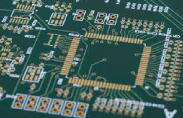
Another critical aspect of HDI PCB design is the implementation of controlled impedance.
Controlled impedance is the characteristic impedance of a transmission line, which must be consistent to prevent signal reflections that can cause data errors. HDI PCBs achieve controlled impedance through precise trace width and spacing, as well as the use of specific materials. This meticulous attention to detail ensures that signals are transmitted with minimal distortion, thereby enhancing the overall performance of the electronic device.
Furthermore, HDI PCBs are designed to minimize electromagnetic interference (EMI), which can significantly impact signal integrity.
EMI is the unwanted disturbance generated by external sources that can affect the performance of electronic circuits. HDI PCBs combat EMI through the use of ground planes and shielding techniques. Ground planes act as a reference point for signals and help in dissipating unwanted noise, while shielding techniques involve enclosing sensitive components in conductive materials to block external interference. These measures are crucial in maintaining the integrity of high-speed signals, especially in densely packed circuits.
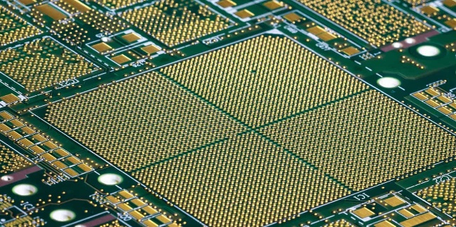
In addition to these design features, the manufacturing process of HDI PCBs also plays a vital role in enhancing signal integrity.
Advanced fabrication techniques, such as laser drilling and sequential lamination, allow for the creation of precise and reliable interconnections. These techniques ensure that the physical structure of the PCB supports optimal signal transmission, thereby reducing the likelihood of signal degradation.
In conclusion, HDI PCBs are instrumental in enhancing signal integrity in modern electronic devices. Through the use of microvias, multiple layers, controlled impedance, and EMI mitigation techniques, these advanced circuit boards ensure that high-speed signals are transmitted accurately and reliably. As the demand for smaller, more powerful electronic devices continues to grow, the importance of HDI PCBs in maintaining signal integrity will only become more pronounced. By leveraging the unique design and manufacturing features of HDI PCBs, designers can create high-performance electronic devices that meet the rigorous demands of today’s technology-driven world.
Applications of HDI PCBs in Medical Devices
High-Density Interconnect (HDI) printed circuit boards (PCBs) have revolutionized the landscape of medical devices, offering unparalleled advantages in terms of miniaturization, performance, and reliability. As the medical field continues to advance, the demand for more compact, efficient, and sophisticated devices has surged, making HDI PCBs an indispensable component in modern medical technology.
One of the primary applications of HDI PCBs in medical devices is in diagnostic equipment.
These devices require high precision and reliability to ensure accurate results. HDI PCBs, with their fine lines and spaces, micro vias, and high connection pad density, enable the creation of compact and highly efficient diagnostic tools. For instance, portable ultrasound machines, which necessitate high-resolution imaging and real-time data processing, benefit significantly from the advanced capabilities of HDI PCBs. The miniaturization afforded by HDI technology allows for the development of handheld devices that are both powerful and easy to use, enhancing the accessibility and convenience of diagnostic procedures.
In addition to diagnostic equipment, HDI PCBs are also crucial in therapeutic devices.
Devices such as pacemakers and implantable defibrillators require a high degree of reliability and longevity, as they are critical to patient health and often operate within the human body for extended periods. The robust construction and high performance of HDI PCBs ensure that these devices function flawlessly, providing consistent and reliable therapeutic interventions. Moreover, the miniaturization capabilities of HDI technology allow for the development of smaller, less invasive devices, which can significantly improve patient comfort and reduce recovery times.
Furthermore, HDI PCBs play a vital role in the development of wearable medical devices.
These devices, which include fitness trackers, continuous glucose monitors, and wearable ECG monitors, require compact and lightweight components to ensure user comfort and convenience. HDI PCBs, with their ability to support high component density and complex circuitry in a small footprint, are ideally suited for these applications. The integration of HDI technology in wearable devices not only enhances their functionality but also enables the incorporation of advanced features such as wireless connectivity and real-time data monitoring, thereby improving patient outcomes and facilitating proactive healthcare management.
Another significant application of HDI PCBs in medical devices is in imaging systems.
Advanced imaging technologies such as MRI and CT scanners rely on high-performance electronics to process large volumes of data quickly and accurately. HDI PCBs, with their superior electrical performance and high-speed signal transmission capabilities, are essential in ensuring the efficiency and accuracy of these imaging systems. The use of HDI technology in imaging devices allows for the development of more compact and efficient systems, which can lead to improved diagnostic capabilities and better patient care.
In conclusion, the applications of HDI PCBs in medical devices are vast and varied, encompassing diagnostic equipment, therapeutic devices, wearable technology, and imaging systems. The unique advantages of HDI technology, including miniaturization, high performance, and reliability, make it an essential component in the advancement of medical technology. As the medical field continues to evolve, the role of HDI PCBs in enabling the development of more sophisticated, efficient, and patient-friendly devices will undoubtedly become even more critical, driving further innovations and improvements in healthcare.
HDI PCBs in Consumer Electronics: Trends and Innovations
High-Density Interconnect (HDI) Printed Circuit Boards (PCBs) have become a cornerstone in the realm of consumer electronics, driving advancements and enabling the creation of increasingly sophisticated devices. As the demand for smaller, faster, and more efficient electronic gadgets continues to surge, HDI PCBs have emerged as a pivotal technology, facilitating the miniaturization and enhanced performance of modern consumer electronics.
One of the most significant trends in the application of HDI PCBs in consumer electronics is the push towards miniaturization.
Modern consumers expect their devices to be compact yet powerful, a demand that has led to the proliferation of HDI technology. By utilizing finer lines and spaces, smaller vias, and higher connection pad density, HDI PCBs allow for more components to be packed into a smaller area. This capability is particularly crucial in the development of smartphones, tablets, and wearable devices, where space is at a premium. Consequently, manufacturers can produce sleeker, more portable devices without compromising on functionality or performance.
In addition to miniaturization, HDI PCBs contribute significantly to the enhancement of device performance. The use of microvias, blind vias, and buried vias in HDI PCBs reduces the signal path length, thereby minimizing signal loss and improving signal integrity. This is especially important in high-speed applications where data transmission rates are critical. For instance, in the realm of high-definition video streaming and gaming, the superior signal integrity provided by HDI PCBs ensures a seamless and lag-free user experience. Moreover, the improved thermal management capabilities of HDI PCBs help in maintaining optimal operating temperatures, thereby enhancing the reliability and longevity of consumer electronics.
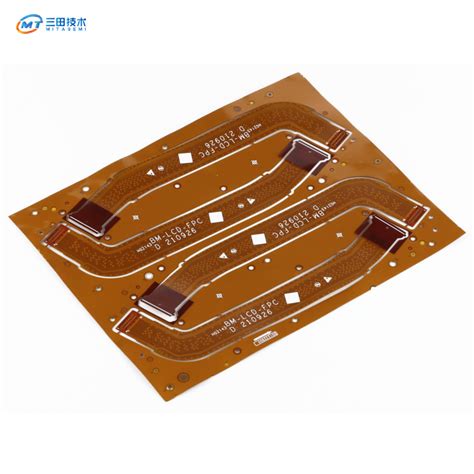
Another noteworthy innovation in the application of HDI PCBs is their role in the development of flexible and rigid-flex PCBs.
These advanced configurations offer greater design flexibility, allowing for the creation of devices with complex shapes and contours. Flexible HDI PCBs are particularly advantageous in wearable technology, where they can conform to the shape of the human body, providing both comfort and functionality. Rigid-flex HDI PCBs, on the other hand, combine the benefits of both rigid and flexible circuits, enabling the design of robust yet adaptable electronic devices. This versatility is driving innovation in various consumer electronics sectors, including medical devices, automotive electronics, and smart home appliances.
Furthermore, the integration of HDI PCBs with advanced materials and manufacturing techniques is paving the way for next-generation consumer electronics.
The use of materials such as liquid crystal polymer (LCP) and polyimide in HDI PCBs enhances their electrical performance and thermal stability. Additionally, advancements in manufacturing processes, such as laser drilling and sequential lamination, are enabling the production of HDI PCBs with even finer features and higher layer counts. These technological advancements are not only improving the performance and reliability of consumer electronics but also reducing production costs and time-to-market.
In conclusion, the application of HDI PCBs in consumer electronics is characterized by trends and innovations that are driving the industry forward. The push towards miniaturization, enhanced device performance, and the development of flexible and rigid-flex configurations are all contributing to the creation of more advanced and user-friendly electronic devices. As technology continues to evolve, HDI PCBs will undoubtedly play a crucial role in shaping the future of consumer electronics, meeting the ever-growing demands for smaller, faster, and more efficient devices.
The Role of HDI PCBs in Automotive Technology
High-Density Interconnect (HDI) Printed Circuit Boards (PCBs) have become a cornerstone in the advancement of automotive technology. As the automotive industry continues to evolve, the demand for more sophisticated, reliable, and compact electronic systems has surged. HDI PCBs, with their ability to support higher wiring density and finer lines and spaces, are uniquely positioned to meet these demands, thereby playing a crucial role in the development of modern vehicles.
One of the primary applications of HDI PCBs in automotive technology is in the realm of advanced driver-assistance systems (ADAS).
These systems, which include features such as adaptive cruise control, lane departure warning, and automatic emergency braking, rely heavily on complex electronic circuits to function effectively. HDI PCBs enable the integration of multiple electronic components in a compact space, thereby enhancing the performance and reliability of ADAS. This integration is essential for processing the vast amounts of data generated by sensors and cameras, ensuring that the vehicle can respond swiftly and accurately to various driving conditions.
Moreover, the role of HDI PCBs extends to the infotainment systems within modern vehicles.
Today’s consumers expect their cars to offer seamless connectivity, high-quality audio, and advanced navigation features. HDI PCBs facilitate the miniaturization of these infotainment systems, allowing manufacturers to pack more functionality into smaller spaces without compromising on performance. This miniaturization is particularly important as it contributes to the overall aesthetic and ergonomic design of the vehicle’s interior, providing a more enjoyable and user-friendly experience for drivers and passengers alike.
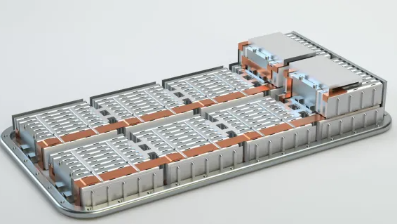
In addition to ADAS and infotainment systems, HDI PCBs are also integral to the development of electric vehicles (EVs). The transition from traditional internal combustion engines to electric powertrains necessitates a complete overhaul of the vehicle’s electronic architecture. HDI PCBs are instrumental in managing the complex power distribution and control systems required for EVs. Their ability to handle higher current densities and provide efficient thermal management ensures that the electronic components within EVs operate reliably and safely. This reliability is crucial for the overall performance and longevity of electric vehicles, making HDI PCBs a vital component in the push towards sustainable transportation.
Furthermore, the integration of HDI PCBs in automotive technology is not limited to passenger vehicles alone. Commercial vehicles, such as trucks and buses, also benefit from the advanced capabilities of HDI PCBs. These vehicles often require robust and reliable electronic systems to manage various functions, including fleet management, telematics, and advanced safety features. HDI PCBs provide the necessary support for these systems, ensuring that commercial vehicles can operate efficiently and safely under demanding conditions.
In conclusion, the role of HDI PCBs in automotive technology is multifaceted and indispensable. Their ability to support higher wiring density, facilitate miniaturization, and enhance reliability makes them a critical component in the development of advanced driver-assistance systems, infotainment systems, electric vehicles, and commercial vehicles. As the automotive industry continues to innovate and push the boundaries of what is possible, the importance of HDI PCBs will only continue to grow, driving further advancements in vehicle technology and contributing to a safer, more connected, and sustainable future.