Hdi pcb design guide
Key Considerations For HDI PCB Design
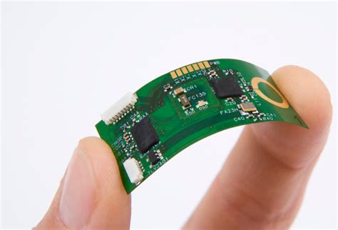
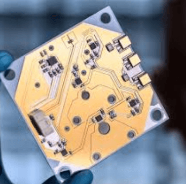
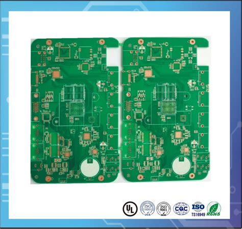
High-Density Interconnect (HDI) printed circuit boards (PCBs) have become increasingly essential in modern electronics due to their ability to support complex circuitry within a compact footprint. As the demand for smaller, faster, and more efficient electronic devices grows, understanding the key considerations for HDI PCB design becomes crucial for engineers and designers. This article delves into the critical aspects that must be taken into account to ensure the successful implementation of HDI technology.
To begin with, one of the primary considerations in HDI PCB design is the selection of materials.
The choice of substrate material significantly impacts the performance, reliability, and manufacturability of the PCB. High-frequency applications, for instance, may require materials with low dielectric constants and low loss tangents to minimize signal degradation. Additionally, thermal management is a vital factor, necessitating materials with good thermal conductivity to dissipate heat effectively. Therefore, careful evaluation of material properties is essential to meet the specific requirements of the application.
Another crucial aspect is the layer stack-up configuration.
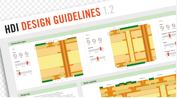
HDI PCBs often incorporate multiple layers to accommodate the dense routing and interconnections required by modern electronic devices. The stack-up design must be meticulously planned to optimize signal integrity, power distribution, and thermal performance. This involves determining the appropriate number of layers, the arrangement of signal, power, and ground planes, and the use of microvias, blind vias, and buried vias to facilitate interlayer connections. Proper stack-up design not only enhances electrical performance but also simplifies the manufacturing process.
Transitioning to the topic of via technology, microvias play a pivotal role in HDI PCB design.
These small-diameter vias enable high-density routing by allowing connections between layers without occupying excessive board space. The use of microvias, however, introduces challenges related to drilling precision and reliability. Laser drilling is commonly employed to create microvias, ensuring high accuracy and consistency. Additionally, the aspect ratio of microvias must be carefully controlled to maintain structural integrity and electrical performance. Designers must also consider the impact of via-in-pad technology, which places vias directly within component pads, reducing signal path lengths and enhancing signal integrity.
Signal integrity is another paramount consideration in HDI PCB design.
As signal frequencies increase, issues such as crosstalk, impedance mismatches, and electromagnetic interference (EMI) become more pronounced. To mitigate these challenges, designers must implement strategies such as controlled impedance routing, differential pair routing, and proper grounding techniques. Additionally, the use of advanced simulation tools can aid in predicting and addressing potential signal integrity issues during the design phase, ensuring optimal performance in the final product.
Power integrity is equally important, as modern electronic devices demand stable and efficient power delivery.
HDI PCBs must incorporate robust power distribution networks (PDNs) to minimize voltage drops and noise. This involves careful placement of decoupling capacitors, strategic routing of power traces, and the use of power planes to provide low-impedance paths for current flow. Effective power integrity design ensures reliable operation and prevents issues such as power supply noise and voltage fluctuations.
Lastly, manufacturability and cost considerations must not be overlooked.
While HDI technology offers numerous benefits, it also introduces complexities in the manufacturing process. Designers must collaborate closely with PCB manufacturers to ensure that the design can be fabricated within acceptable tolerances and yield rates. Factors such as minimum trace widths, spacing, and via sizes must align with the capabilities of the chosen manufacturing process. Additionally, cost implications should be evaluated, as HDI PCBs can be more expensive to produce compared to traditional PCBs. Balancing performance requirements with manufacturability and cost constraints is essential for a successful HDI PCB design.
In conclusion, HDI PCB design demands careful attention to material selection, layer stack-up configuration, via technology, signal and power integrity, and manufacturability. By addressing these key considerations, designers can harness the full potential of HDI technology to create high-performance, reliable, and compact electronic devices that meet the ever-evolving demands of the industry.
Advanced Techniques In HDI PCB Layout
High-Density Interconnect (HDI) printed circuit boards (PCBs) have become a cornerstone in the development of modern electronic devices, offering enhanced performance and miniaturization. As the demand for more compact and efficient electronic products continues to grow, mastering advanced techniques in HDI PCB layout becomes increasingly crucial.
One of the primary techniques involves the use of microvias, which are significantly smaller than traditional vias.
These microvias enable designers to create more intricate and compact layouts by allowing for higher component density and more efficient routing. By employing laser drilling technology, microvias can be precisely placed, thereby optimizing the available space on the PCB.
Another advanced technique is the implementation of sequential lamination.
This process involves multiple layers of dielectric material and copper, which are laminated together in a specific sequence. Sequential lamination allows for the creation of complex multilayer PCBs with improved electrical performance and reliability. This technique is particularly beneficial in applications where signal integrity and high-speed data transmission are critical. Additionally, the use of blind and buried vias in conjunction with sequential lamination can further enhance the routing capabilities and overall performance of the HDI PCB.
Signal integrity is a paramount consideration in HDI PCB design, and controlled impedance is a technique that addresses this concern.
By carefully designing the trace width, spacing, and dielectric material properties, designers can ensure that the impedance of the signal traces remains consistent. This consistency is vital for maintaining signal quality and preventing issues such as signal reflection and crosstalk. Moreover, the use of differential pairs, where two signal traces are routed together with a specific spacing, can further improve signal integrity by reducing electromagnetic interference.
Thermal management is another critical aspect of HDI PCB design, especially as electronic devices become more powerful and generate more heat.
Advanced techniques such as the use of thermal vias and heat sinks can help dissipate heat more effectively, ensuring the longevity and reliability of the PCB. Thermal vias, which are filled or plated with conductive material, provide a direct path for heat to travel from the surface of the PCB to the inner layers or to an external heat sink. This technique is particularly useful in high-power applications where efficient heat dissipation is essential.
Furthermore, the integration of embedded components within the PCB substrate is an emerging technique that offers significant advantages in terms of space savings and performance. By embedding passive components such as resistors and capacitors within the PCB layers, designers can reduce the overall size of the board and improve electrical performance by minimizing parasitic effects. This technique also allows for greater design flexibility and can lead to more robust and reliable PCBs.
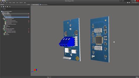
In addition to these techniques, the use of advanced simulation and modeling tools is indispensable in HDI PCB design. These tools enable designers to predict and analyze the electrical, thermal, and mechanical behavior of the PCB before it is manufactured. By simulating various design scenarios, potential issues can be identified and addressed early in the design process, thereby reducing the risk of costly revisions and ensuring a more efficient design cycle.
In conclusion, advanced techniques in HDI PCB layout, such as the use of microvias, sequential lamination, controlled impedance, thermal management, embedded components, and advanced simulation tools, are essential for meeting the demands of modern electronic devices. By mastering these techniques, designers can create more compact, efficient, and reliable PCBs that meet the ever-evolving requirements of the electronics industry.
Benefits Of Using HDI Technology In PCB Design
High-Density Interconnect (HDI) technology has revolutionized the field of printed circuit board (PCB) design, offering a multitude of benefits that cater to the ever-evolving demands of modern electronics. As electronic devices become increasingly compact and complex, the need for efficient and reliable PCB solutions has never been more critical. HDI technology addresses these needs by providing a range of advantages that enhance the performance, functionality, and manufacturability of PCBs.
One of the primary benefits of using HDI technology in PCB design is the significant reduction in size and weight.
Traditional PCBs often struggle to accommodate the growing number of components required for advanced electronic devices. HDI technology, however, utilizes finer lines and spaces, smaller vias, and higher connection pad density, allowing for more components to be placed in a smaller area. This miniaturization is particularly beneficial for portable devices such as smartphones, tablets, and wearable technology, where space is at a premium.
In addition to size reduction, HDI technology also improves the electrical performance of PCBs.
The shorter distances between components and the use of microvias reduce signal loss and electromagnetic interference (EMI), leading to faster signal transmission and enhanced overall performance. This is especially important in high-speed applications where signal integrity is paramount. Furthermore, the improved thermal management capabilities of HDI PCBs help dissipate heat more effectively, ensuring the longevity and reliability of electronic devices.
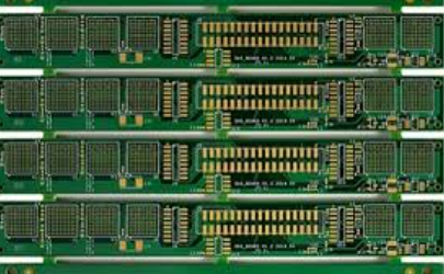
Another notable advantage of HDI technology is its ability to support higher layer counts in multilayer PCBs.
Traditional PCBs with numerous layers can become bulky and difficult to manufacture. HDI technology, with its advanced fabrication techniques, allows for the creation of complex multilayer boards with thinner profiles. This not only saves space but also reduces the overall weight of the PCB, making it ideal for applications where weight is a critical factor, such as aerospace and medical devices.
Moreover, HDI technology enhances the design flexibility of PCBs.
The ability to incorporate blind and buried vias, as well as via-in-pad structures, provides designers with more options to route traces and place components. This flexibility is crucial for optimizing the layout and achieving the desired electrical performance. Additionally, the use of advanced materials and manufacturing processes in HDI technology enables the production of PCBs with higher reliability and durability, which is essential for applications that require long-term performance and dependability.
The benefits of HDI technology extend beyond the technical aspects of PCB design.
From a manufacturing perspective, HDI PCBs can lead to cost savings in the long run. Although the initial design and fabrication costs may be higher due to the advanced techniques and materials used, the overall reduction in size, weight, and component count can result in lower assembly and shipping costs. Furthermore, the improved performance and reliability of HDI PCBs can reduce the need for repairs and replacements, leading to cost savings over the product’s lifecycle.
In conclusion, HDI technology offers a myriad of benefits that make it an indispensable tool in modern PCB design. The ability to reduce size and weight, improve electrical performance, support higher layer counts, enhance design flexibility, and achieve cost savings underscores the value of HDI technology in meeting the demands of contemporary electronic devices. As the electronics industry continues to push the boundaries of innovation, HDI technology will undoubtedly play a pivotal role in shaping the future of PCB design.
Common Challenges And Solutions In HDI PCB Design
High-Density Interconnect (HDI) Printed Circuit Boards (PCBs) have become increasingly prevalent in modern electronics due to their ability to support complex circuitry within a compact footprint. However, designing HDI PCBs presents several challenges that require careful consideration and strategic solutions.
One of the primary challenges in HDI PCB design is managing the intricate routing of traces.
As the density of components increases, the available space for routing decreases, making it difficult to maintain signal integrity. To address this, designers often employ advanced techniques such as microvias, blind and buried vias, and via-in-pad technology. These methods allow for more efficient use of space and help in maintaining the necessary electrical performance.
Another significant challenge is thermal management.
With the miniaturization of components and the increased power density, effective heat dissipation becomes crucial. Inadequate thermal management can lead to overheating, which can compromise the reliability and longevity of the PCB. To mitigate this issue, designers can use thermal vias, heat sinks, and thermal pads to enhance heat dissipation. Additionally, selecting materials with high thermal conductivity for the PCB substrate can further improve thermal performance.
Signal integrity is also a critical concern in HDI PCB design.
High-speed signals are more susceptible to issues such as crosstalk, electromagnetic interference (EMI), and signal attenuation. To ensure signal integrity, designers must carefully plan the layout, considering factors such as trace width, spacing, and impedance control. Utilizing differential pairs and proper grounding techniques can help minimize crosstalk and EMI. Moreover, incorporating signal integrity analysis tools during the design phase can aid in identifying and addressing potential issues before fabrication.
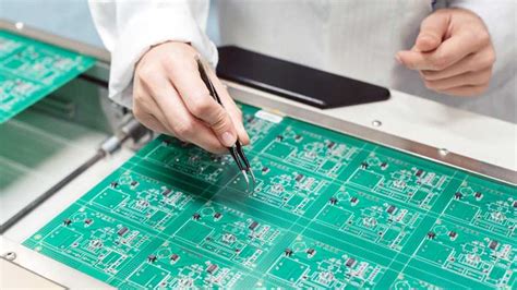
The manufacturing process of HDI PCBs poses its own set of challenges.
The precision required for drilling microvias and the alignment of multiple layers necessitate advanced fabrication techniques. Ensuring the reliability of these processes is essential to prevent defects such as misalignment, voids, and delamination. Collaborating closely with experienced PCB manufacturers and adhering to their design guidelines can significantly reduce the risk of manufacturing defects. Furthermore, conducting thorough design for manufacturability (DFM) reviews can help identify potential issues early in the design process.
Material selection is another critical aspect that can impact the performance and reliability of HDI PCBs.
The choice of materials affects factors such as signal integrity, thermal management, and mechanical stability. High-frequency applications, for instance, require materials with low dielectric constant and low loss tangent to minimize signal loss. Additionally, the coefficient of thermal expansion (CTE) of the materials should be compatible with the components to prevent mechanical stress during thermal cycling. Collaborating with material suppliers to select the appropriate materials for specific applications can enhance the overall performance of the HDI PCB.
Finally, testing and validation are essential steps in ensuring the functionality and reliability of HDI PCBs.
Given the complexity of these designs, traditional testing methods may not be sufficient. Advanced testing techniques such as automated optical inspection (AOI), X-ray inspection, and in-circuit testing (ICT) can help identify defects and verify the performance of the PCB. Implementing a comprehensive testing strategy throughout the design and manufacturing process can significantly reduce the risk of failures in the final product.
In conclusion, while HDI PCB design presents several challenges, strategic solutions and careful planning can effectively address these issues. By employing advanced routing techniques, ensuring proper thermal management, maintaining signal integrity, collaborating with experienced manufacturers, selecting appropriate materials, and implementing thorough testing procedures, designers can successfully navigate the complexities of HDI PCB design and deliver reliable, high-performance products.