Hdi pcb europe
Advancements In HDI PCB Manufacturing Technologies In Europe
High-Density Interconnect (HDI) printed circuit boards (PCBs) have become a cornerstone in the evolution of modern electronics, offering enhanced performance and miniaturization capabilities.
In Europe, advancements in HDI PCB manufacturing technologies are driving significant progress in various industries, including telecommunications, automotive, and consumer electronics. As the demand for more compact and efficient electronic devices continues to rise, European manufacturers are at the forefront of developing innovative solutions to meet these needs.
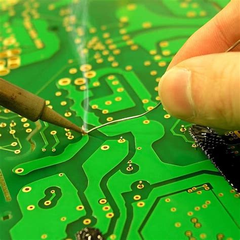
One of the key advancements in HDI PCB manufacturing in Europe is the adoption of laser drilling technology.
This technique allows for the creation of microvias, which are essential for the high-density interconnects that characterize HDI PCBs. Laser drilling offers precision and efficiency, enabling manufacturers to produce smaller and more complex circuit boards. This advancement not only enhances the electrical performance of the PCBs but also reduces their size, which is crucial for applications in compact devices such as smartphones and wearable technology.
Moreover, European manufacturers are increasingly utilizing advanced materials to improve the performance and reliability of HDI PCBs.
The use of high-performance laminates and substrates, such as polyimide and liquid crystal polymer, provides better thermal management and signal integrity. These materials are particularly beneficial in applications that require high-speed data transmission and operate in harsh environments. By integrating these advanced materials, European manufacturers are able to produce HDI PCBs that meet the stringent requirements of modern electronic devices.
In addition to material advancements, the implementation of sophisticated design software has revolutionized the HDI PCB manufacturing process in Europe.
Computer-aided design (CAD) tools enable engineers to create intricate PCB layouts with precision and efficiency. These tools facilitate the optimization of layer stack-ups, trace routing, and via placement, ensuring that the final product meets the desired specifications. The integration of simulation software further allows for the testing and validation of designs before they are physically manufactured, reducing the risk of errors and improving overall product quality.
Furthermore, the European HDI PCB industry is benefiting from the adoption of Industry 4.0 technologies, which are transforming traditional manufacturing processes.
Automation and robotics are being increasingly employed to enhance production efficiency and consistency. Automated optical inspection (AOI) systems, for instance, are used to detect defects in PCBs with high accuracy, ensuring that only high-quality products reach the market. Additionally, the use of data analytics and machine learning algorithms is enabling manufacturers to optimize production processes and predict maintenance needs, thereby reducing downtime and costs.
As environmental concerns continue to gain prominence, European HDI PCB manufacturers are also focusing on sustainable practices.
The development of lead-free soldering techniques and the use of environmentally friendly materials are becoming standard practices in the industry. These efforts not only align with regulatory requirements but also cater to the growing consumer demand for eco-friendly products.
In conclusion, the advancements in HDI PCB manufacturing technologies in Europe are paving the way for the next generation of electronic devices. Through the adoption of laser drilling, advanced materials, sophisticated design software, and Industry 4.0 technologies, European manufacturers are enhancing the performance, reliability, and sustainability of HDI PCBs. As these technologies continue to evolve, Europe is poised to remain a leader in the global HDI PCB market, driving innovation and meeting the ever-increasing demands of the electronics industry.

The Role Of HDI PCBs In The European Electronics Industry
High-Density Interconnect (HDI) printed circuit boards (PCBs) have become a cornerstone in the European electronics industry, playing a pivotal role in advancing technology and innovation. As the demand for more compact, efficient, and powerful electronic devices continues to rise, HDI PCBs have emerged as a critical component in meeting these needs. Their ability to support higher wiring density and finer lines and spaces makes them indispensable in the development of modern electronic products.
In Europe, the electronics industry is a significant contributor to the economy, with sectors such as telecommunications, automotive, aerospace, and consumer electronics relying heavily on advanced PCB technologies.
HDI PCBs, with their multilayer configurations and microvia technology, enable the miniaturization of electronic devices without compromising performance. This is particularly important in the European market, where there is a strong emphasis on innovation and sustainability. By allowing for more components to be packed into a smaller area, HDI PCBs contribute to the development of lighter and more energy-efficient devices, aligning with Europe’s environmental goals.
Moreover, the integration of HDI PCBs in the automotive industry is noteworthy.
As Europe leads the charge in the transition to electric vehicles (EVs), the need for sophisticated electronic systems has surged. HDI PCBs are crucial in this context, as they support the complex circuitry required for battery management systems, advanced driver-assistance systems (ADAS), and infotainment systems. The ability of HDI PCBs to handle high-speed signals and power distribution efficiently makes them ideal for the automotive sector, where reliability and performance are paramount.
In addition to automotive applications, the telecommunications industry in Europe also benefits significantly from HDI PCB technology.
With the rollout of 5G networks, there is an increased demand for high-performance networking equipment. HDI PCBs facilitate the development of compact and efficient communication devices that can handle the high data rates and low latency required by 5G technology. This advancement not only enhances connectivity but also supports the growth of the Internet of Things (IoT), which is rapidly expanding across Europe.
Furthermore, the aerospace industry, known for its stringent requirements and high standards, relies on HDI PCBs for mission-critical applications.
The ability to withstand harsh environments and deliver reliable performance is essential in aerospace electronics. HDI PCBs, with their robust design and high reliability, meet these demands, making them a preferred choice for avionics and satellite systems.
As the European electronics industry continues to evolve, the role of HDI PCBs is expected to grow even more significant.
The ongoing research and development efforts in Europe aim to push the boundaries of HDI technology, exploring new materials and manufacturing processes to further enhance performance and reduce costs. This commitment to innovation ensures that Europe remains at the forefront of the global electronics market.
In conclusion, HDI PCBs are integral to the European electronics industry, driving advancements across various sectors. Their ability to support miniaturization, improve performance, and enhance reliability makes them a vital component in the development of cutting-edge electronic devices. As Europe continues to prioritize innovation and sustainability, the importance of HDI PCBs is likely to increase, solidifying their role as a key enabler of technological progress.
Challenges And Opportunities For HDI PCB Designers In Europe
The landscape of High-Density Interconnect (HDI) Printed Circuit Board (PCB) design in Europe is marked by a unique set of challenges and opportunities that are shaping the future of the electronics industry. As the demand for more compact, efficient, and high-performance electronic devices continues to grow, HDI PCBs have become increasingly crucial.
These advanced circuit boards, characterized by their finer lines and spaces, smaller vias, and higher connection pad density, are essential for modern electronic devices. However, designing HDI PCBs in Europe presents several challenges that designers must navigate to remain competitive in the global market.
One of the primary challenges faced by HDI PCB designers in Europe is the rapid pace of technological advancement.
As technology evolves, so too do the requirements for PCBs. Designers must constantly update their skills and knowledge to keep up with the latest trends and innovations. This requires a commitment to continuous learning and adaptation, which can be resource-intensive. Moreover, the complexity of HDI PCB design necessitates the use of advanced design tools and software, which can be costly and require significant investment from companies.
In addition to technological challenges, European HDI PCB designers must also contend with stringent regulatory standards.
The European Union has some of the most rigorous environmental and safety regulations in the world, which can impact the materials and processes used in PCB manufacturing. Designers must ensure that their products comply with these regulations, which can add an additional layer of complexity to the design process. This often involves working closely with manufacturers to ensure that all components and materials meet the necessary standards.
Despite these challenges, there are significant opportunities for HDI PCB designers in Europe.
The region is home to a robust electronics industry, with a strong emphasis on innovation and quality. European designers have the opportunity to leverage this reputation to attract global clients who are seeking high-quality, reliable products. Furthermore, the growing demand for advanced electronic devices in sectors such as automotive, aerospace, and telecommunications presents a wealth of opportunities for HDI PCB designers. These industries require increasingly sophisticated PCBs to support the development of cutting-edge technologies, such as autonomous vehicles and 5G networks.
Another opportunity lies in the growing trend towards sustainability in electronics design.
As consumers and businesses become more environmentally conscious, there is a rising demand for sustainable and eco-friendly products. HDI PCB designers in Europe can capitalize on this trend by developing innovative solutions that reduce waste and energy consumption. This not only aligns with European regulatory standards but also positions designers as leaders in sustainable technology.
In conclusion, while HDI PCB designers in Europe face a range of challenges, from keeping pace with technological advancements to navigating complex regulatory environments, there are also numerous opportunities to be seized. By embracing innovation, focusing on quality, and prioritizing sustainability, European designers can not only overcome these challenges but also thrive in the competitive global market. As the demand for advanced electronic devices continues to grow, those who can successfully navigate this landscape will be well-positioned to lead the industry into the future.
Sustainability Practices In European HDI PCB Production
In recent years, the European high-density interconnect (HDI) printed circuit board (PCB) industry has increasingly prioritized sustainability, reflecting a broader commitment to environmental responsibility. This shift is driven by both regulatory pressures and a growing awareness of the environmental impact of electronic manufacturing. As a result, European HDI PCB producers are adopting a range of sustainable practices aimed at minimizing their ecological footprint while maintaining high standards of quality and innovation.
One of the primary strategies employed by European HDI PCB manufacturers is the implementation of energy-efficient production processes.
By investing in state-of-the-art machinery and optimizing production lines, these companies are able to significantly reduce energy consumption. For instance, the use of advanced laser drilling techniques not only enhances precision but also decreases the energy required compared to traditional mechanical drilling methods. Additionally, many facilities are transitioning to renewable energy sources, such as solar or wind power, to further diminish their reliance on fossil fuels.
Moreover, the European HDI PCB industry is making strides in reducing waste and promoting recycling.
The adoption of closed-loop systems allows manufacturers to recycle materials such as copper and other metals, which are integral to PCB production. By reclaiming these materials, companies can decrease the demand for virgin resources and reduce the environmental impact associated with mining and processing. Furthermore, the use of water treatment systems ensures that water used in the manufacturing process is purified and reused, thereby conserving this vital resource.
In addition to these efforts, European HDI PCB producers are increasingly focusing on the use of environmentally friendly materials.
The shift towards lead-free soldering, driven by the Restriction of Hazardous Substances (RoHS) directive, exemplifies this commitment. By eliminating lead and other hazardous substances from their products, manufacturers not only comply with regulatory requirements but also contribute to a safer and more sustainable environment. Additionally, the development of biodegradable and recyclable substrate materials is gaining traction, offering a promising avenue for reducing the long-term environmental impact of PCBs.
Collaboration and innovation are also key components of sustainability practices in the European HDI PCB sector.
Many companies are partnering with research institutions and industry organizations to develop new technologies and processes that enhance sustainability. These collaborations often result in the creation of industry standards and best practices that guide manufacturers in their sustainability efforts. Furthermore, by sharing knowledge and resources, companies can accelerate the adoption of sustainable practices across the industry.
The commitment to sustainability in European HDI PCB production is further reinforced by the increasing demand from consumers and clients for environmentally responsible products.
As awareness of environmental issues grows, customers are more inclined to choose products that align with their values. This shift in consumer preferences is encouraging manufacturers to prioritize sustainability as a core aspect of their business strategy, thereby driving continuous improvement in environmental performance.
In conclusion, the European HDI PCB industry is making significant progress in adopting sustainability practices that reduce environmental impact while maintaining high standards of quality and innovation. Through energy-efficient production processes, waste reduction and recycling initiatives, the use of environmentally friendly materials, and collaborative efforts, the industry is setting a benchmark for sustainable manufacturing. As these practices continue to evolve, they will play a crucial role in shaping a more sustainable future for the electronics industry as a whole.


