Heavy Copper PCB: Design, Applications, and Manufacturing Considerations
Introduction
Printed Circuit Boards (PCBs) are the backbone of modern electronics, providing the necessary electrical connections and mechanical support for electronic components. As technology advances, the demand for PCBs capable of handling higher currents, dissipating more heat, and enduring harsh environments has grown significantly. This has led to the development and widespread adoption of Heavy Copper PCBs, a specialized type of PCB that incorporates thicker copper layers than standard boards. This article explores the design, applications, and manufacturing considerations of Heavy Copper PCBs, providing a comprehensive overview of this critical technology.
What is Heavy Copper PCB?
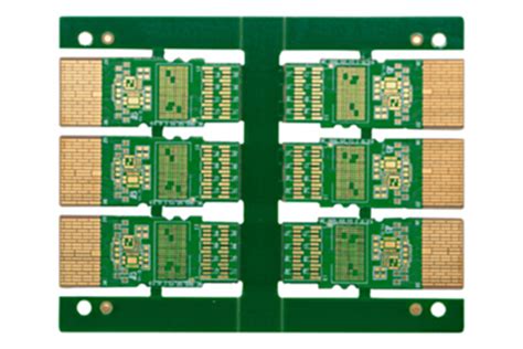
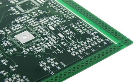
Heavy Copper PCBs are characterized by their use of copper layers that are significantly thicker than those found in standard PCBs. While standard PCBs typically use copper layers with thicknesses ranging from 1 oz (35 µm) to 3 oz (105 µm), Heavy Copper PCBs employ copper layers that can range from 4 oz (140 µm) to 20 oz (700 µm) or more. The increased copper thickness allows these boards to carry higher currents, improve thermal management, and enhance mechanical strength.
Design Considerations for Heavy Copper PCBs
Designing Heavy Copper PCBs requires careful consideration of several factors to ensure optimal performance and manufacturability. Key design considerations include:
- Current Carrying Capacity: The primary advantage of Heavy Copper PCBs is their ability to carry higher currents. Designers must calculate the required current carrying capacity and select the appropriate copper thickness to minimize resistive losses and prevent overheating. Tools like IPC-2152 standards can help determine the necessary trace widths and copper weights for a given current.
- Thermal Management: Heavy Copper PCBs are often used in high-power applications where heat dissipation is critical. The increased copper thickness improves thermal conductivity, allowing heat to be more effectively transferred away from heat-generating components. Designers should incorporate thermal vias, heat sinks, and other cooling mechanisms to further enhance thermal performance.
- Mechanical Strength: The additional copper layers in Heavy Copper PCBs provide increased mechanical strength, making them suitable for applications subject to mechanical stress or vibration. Designers should consider the mechanical requirements of the application and ensure that the PCB layout and material selection can withstand the expected stresses.
- Layer Stackup: Heavy Copper PCBs often require a modified layer stackup to accommodate the thicker copper layers. Designers must work closely with manufacturers to ensure that the layer stackup is optimized for both electrical performance and manufacturability. This may involve adjusting the dielectric thicknesses and selecting appropriate materials to maintain impedance control and signal integrity.
- Etching and Plating: The etching and plating processes for Heavy Copper PCBs are more complex than those for standard PCBs. Designers must account for the challenges associated with etching thicker copper layers, such as undercutting and sidewall plating. Proper design rules, such as increased trace spacing and larger via sizes, can help mitigate these issues.
Applications of Heavy Copper PCBs
Heavy Copper PCBs are used in a wide range of applications where high current carrying capacity, thermal management, and mechanical strength are critical. Some of the most common applications include:
- Power Electronics: Heavy Copper PCBs are widely used in power electronics, such as power supplies, inverters, and motor controllers. These applications require PCBs capable of handling high currents and dissipating significant amounts of heat, making Heavy Copper PCBs an ideal choice.
- Automotive: The automotive industry relies on Heavy Copper PCBs for various applications, including engine control units (ECUs), battery management systems (BMS), and LED lighting. The harsh operating conditions in automotive environments, such as high temperatures and vibrations, necessitate the use of robust PCBs with enhanced thermal and mechanical properties.
- Aerospace and Defense: Heavy Copper PCBs are used in aerospace and defense applications where reliability and performance are paramount. These PCBs are found in avionics, radar systems, and communication equipment, where they must withstand extreme temperatures, shock, and vibration.
- Industrial Equipment: Heavy Copper PCBs are commonly used in industrial equipment, such as welding machines, industrial robots, and power distribution systems. These applications often involve high-power components and require PCBs that can handle high currents and dissipate heat effectively.
- Renewable Energy: The renewable energy sector, including solar and wind power systems, relies on Heavy Copper PCBs for power conversion and distribution. These PCBs are used in inverters, charge controllers, and battery management systems, where they must handle high currents and operate reliably in challenging environments.
Manufacturing Considerations for Heavy Copper PCBs
The manufacturing process for Heavy Copper PCBs presents unique challenges that require specialized techniques and equipment. Key manufacturing considerations include:
- Material Selection: The choice of materials is critical for Heavy Copper PCBs. High-quality base materials, such as FR-4, polyimide, or ceramic-filled PTFE, are often used to ensure good thermal and mechanical properties. The dielectric materials must be compatible with the thicker copper layers and capable of withstanding the higher temperatures associated with heavy copper plating and etching.
- Copper Plating: The plating process for Heavy Copper PCBs involves depositing thicker layers of copper onto the substrate. This requires precise control of plating parameters, such as current density, bath chemistry, and plating time, to achieve uniform copper thickness and avoid defects like voids or nodules.
- Etching: Etching thicker copper layers is more challenging than etching standard copper layers. The etching process must be carefully controlled to avoid undercutting, where the etchant removes more copper from the sides of the traces than intended. This can lead to reduced trace widths and compromised electrical performance. Advanced etching techniques, such as differential etching, may be employed to achieve the desired trace geometries.
- Drilling and Via Formation: Drilling holes and forming vias in Heavy Copper PCBs require specialized equipment and techniques. The thicker copper layers can cause drill bit wear and require slower drilling speeds to prevent damage to the PCB. Additionally, the plating of vias in Heavy Copper PCBs must be carefully managed to ensure good electrical connectivity and mechanical strength.
- Surface Finish: The surface finish of Heavy Copper PCBs must be chosen to provide good solderability, corrosion resistance, and electrical performance. Common surface finishes for Heavy Copper PCBs include HASL (Hot Air Solder Leveling), ENIG (Electroless Nickel Immersion Gold), and OSP (Organic Solderability Preservative). The choice of surface finish depends on the specific application and manufacturing requirements.
- Inspection and Testing: Heavy Copper PCBs require rigorous inspection and testing to ensure quality and reliability. Automated optical inspection (AOI), X-ray inspection, and electrical testing are commonly used to detect defects such as shorts, opens, and insufficient plating. Thermal testing may also be performed to verify the PCB’s ability to dissipate heat effectively.
Advantages and Disadvantages of Heavy Copper PCBs
Heavy Copper PCBs offer several advantages over standard PCBs, but they also come with some disadvantages that must be considered.
Advantages:
- High Current Carrying Capacity: The primary advantage of Heavy Copper PCBs is their ability to carry higher currents, making them suitable for high-power applications.
- Improved Thermal Management: The increased copper thickness enhances thermal conductivity, allowing for better heat dissipation and improved thermal performance.
- Enhanced Mechanical Strength: Heavy Copper PCBs are more robust and can withstand mechanical stress and vibration better than standard PCBs.
- Space Savings: By allowing for higher current carrying capacity in a smaller footprint, Heavy Copper PCBs can reduce the overall size of electronic assemblies.
- Reliability: Heavy Copper PCBs are more reliable in harsh environments, making them ideal for applications in automotive, aerospace, and industrial sectors.
Disadvantages:
- Higher Cost: The increased material costs and more complex manufacturing processes make Heavy Copper PCBs more expensive than standard PCBs.
- Design Complexity: Designing Heavy Copper PCBs requires specialized knowledge and careful consideration of factors such as current carrying capacity, thermal management, and manufacturability.
- Manufacturing Challenges: The manufacturing process for Heavy Copper PCBs is more complex and requires specialized equipment and techniques, which can lead to longer lead times and higher production costs.
- Weight: The increased copper thickness adds weight to the PCB, which may be a concern in weight-sensitive applications such as aerospace.
Future Trends in Heavy Copper PCB Technology
As the demand for high-power and high-reliability electronics continues to grow, Heavy Copper PCB technology is expected to evolve to meet new challenges and opportunities. Some of the key trends in Heavy Copper PCB technology include:
- Advanced Materials: The development of new materials with improved thermal and electrical properties will enable the production of Heavy Copper PCBs with even higher performance. Materials such as ceramic-filled PTFE and advanced polyimides are being explored for use in Heavy Copper PCBs.
- Miniaturization: As electronic devices become smaller and more compact, there is a growing need for Heavy Copper PCBs that can deliver high current carrying capacity in a smaller footprint. Advances in manufacturing techniques, such as laser drilling and precision etching, will enable the production of more compact Heavy Copper PCBs.
- Integration with Other Technologies: Heavy Copper PCBs are increasingly being integrated with other technologies, such as embedded components and flexible circuits, to create more complex and versatile electronic assemblies. This trend is expected to continue, driven by the need for more compact and multifunctional electronic devices.
- Sustainability: As environmental concerns become more prominent, there is a growing focus on developing sustainable manufacturing processes for Heavy Copper PCBs. This includes the use of eco-friendly materials, recycling of copper, and reducing the environmental impact of the manufacturing process.
Conclusion
Heavy Copper PCBs are a critical technology for high-power and high-reliability applications, offering significant advantages in terms of current carrying capacity, thermal management, and mechanical strength. However, the design and manufacturing of Heavy Copper PCBs present unique challenges that require specialized knowledge and techniques. As technology continues to advance, Heavy Copper PCB technology is expected to evolve, driven by the demand for more compact, reliable, and sustainable electronic devices. By understanding the design, applications, and manufacturing considerations of Heavy Copper PCBs, engineers and designers can leverage this technology to create innovative solutions for a wide range of industries.


