Heavy copper pcb thickness
Understanding The Benefits Of Heavy Copper PCB Thickness In Power Electronics
In the realm of power electronics, the significance of heavy copper printed circuit boards (PCBs) cannot be overstated. These specialized PCBs are characterized by their increased copper thickness, which typically ranges from 3 ounces per square foot (oz/ft²) to 20 oz/ft² or more. This enhanced thickness offers a multitude of benefits that are particularly advantageous in high-power applications. As we delve into the advantages of heavy copper PCB thickness, it becomes evident that these benefits are pivotal in optimizing the performance and reliability of power electronic devices.
To begin with, one of the primary advantages of heavy copper PCBs is their ability to handle higher current loads.
The increased copper thickness allows for wider and thicker traces, which can carry more current without overheating. This is crucial in power electronics, where devices often operate under high current conditions. By effectively managing these currents, heavy copper PCBs help in reducing the risk of circuit failure due to overheating, thereby enhancing the overall reliability of the electronic device.
Moreover, heavy copper PCBs exhibit superior thermal management capabilities.
The thicker copper layers facilitate better heat dissipation, which is essential in preventing thermal buildup that can lead to component damage. This is particularly important in applications such as power converters, motor controllers, and power distribution systems, where efficient heat management is critical to maintaining optimal performance. By dissipating heat more effectively, heavy copper PCBs contribute to the longevity and stability of power electronic systems.
In addition to improved current handling and thermal management, heavy copper PCBs also offer enhanced mechanical strength.
The robust nature of these PCBs makes them more resistant to mechanical stresses, such as those encountered during assembly and operation. This increased durability is beneficial in environments where electronic devices are subject to harsh conditions, including vibration and physical impact. Consequently, heavy copper PCBs are often the preferred choice in industrial and automotive applications, where reliability and durability are paramount.
Furthermore, the use of heavy copper PCBs can lead to more compact and efficient designs.
The ability to carry higher currents and dissipate heat more effectively allows for the integration of more components into a smaller area without compromising performance. This is particularly advantageous in modern electronic devices, where space is often at a premium. By enabling more compact designs, heavy copper PCBs facilitate the development of smaller, more efficient power electronic systems.
Additionally, heavy copper PCBs provide greater design flexibility.
The increased thickness allows for the incorporation of complex circuit patterns and multilayer designs, which can accommodate a wide range of functionalities. This flexibility is essential in meeting the diverse requirements of power electronic applications, from simple power distribution to complex control systems. As a result, designers can create more sophisticated and efficient electronic solutions tailored to specific needs.
In conclusion, the benefits of heavy copper PCB thickness in power electronics are manifold.
From improved current handling and thermal management to enhanced mechanical strength and design flexibility, these PCBs play a crucial role in optimizing the performance and reliability of power electronic devices. As the demand for more efficient and compact electronic solutions continues to grow, the importance of heavy copper PCBs in meeting these challenges becomes increasingly apparent. By leveraging the advantages of heavy copper PCB thickness, designers and engineers can develop innovative power electronic systems that meet the rigorous demands of modern applications.

Design Considerations For Heavy Copper PCB Thickness In High-Current Applications
In the realm of high-current applications, the design considerations for heavy copper printed circuit boards (PCBs) are of paramount importance. These specialized PCBs, characterized by their increased copper thickness, are engineered to handle higher current loads and dissipate heat more effectively than standard PCBs. As the demand for more robust and reliable electronic devices continues to grow, understanding the intricacies of heavy copper PCB thickness becomes essential for engineers and designers.
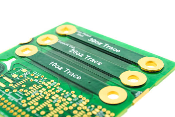
To begin with, heavy copper PCBs are defined by their copper thickness, which typically ranges from 3 ounces per square foot (oz/ft²) to 20 oz/ft² or more.
This increased thickness allows the PCB to conduct higher currents without overheating, making them ideal for applications such as power supplies, automotive electronics, and industrial control systems. The ability to handle high current loads is crucial in these applications, as it ensures the stability and longevity of the electronic components involved.
Moreover, the thermal management capabilities of heavy copper PCBs are significantly enhanced due to their increased copper thickness.
In high-current applications, excessive heat generation can lead to component failure and reduced performance. Heavy copper PCBs mitigate this risk by providing a more efficient heat dissipation pathway, thereby maintaining optimal operating temperatures. This is particularly important in environments where temperature fluctuations are common, as it helps prevent thermal stress and prolongs the lifespan of the device.
In addition to thermal management, the mechanical strength of heavy copper PCBs is another critical consideration.
The thicker copper layers contribute to the overall durability of the PCB, making it more resistant to mechanical stresses such as bending and vibration. This is especially beneficial in applications where the PCB may be subjected to harsh conditions or frequent handling. The enhanced mechanical strength ensures that the PCB maintains its structural integrity, thereby reducing the likelihood of failure due to physical damage.
Furthermore, the design of heavy copper PCBs must account for the increased weight and size associated with thicker copper layers.
This can impact the overall design and layout of the PCB, as well as the choice of materials used in its construction. Designers must carefully balance the need for increased copper thickness with the constraints of space and weight, ensuring that the final product meets the specific requirements of the application. This often involves a detailed analysis of the current-carrying capacity, thermal performance, and mechanical properties of the PCB.
Transitioning to the manufacturing process, it is important to note that the production of heavy copper PCBs requires specialized techniques and equipment.
The increased copper thickness necessitates the use of advanced etching and plating processes to ensure precise and accurate results. Manufacturers must also consider the potential for increased production costs and lead times, as these factors can impact the overall feasibility of the project. By collaborating closely with experienced PCB manufacturers, designers can optimize the production process and achieve the desired balance between performance and cost.
In conclusion, the design considerations for heavy copper PCB thickness in high-current applications are multifaceted and require a comprehensive understanding of the interplay between electrical, thermal, and mechanical factors. By carefully evaluating these aspects, designers can create PCBs that not only meet the demands of high-current applications but also deliver reliable and long-lasting performance. As technology continues to advance, the role of heavy copper PCBs in powering the next generation of electronic devices will undoubtedly become even more significant.
Comparing Heavy Copper PCB Thickness With Standard PCB Thickness
In the realm of printed circuit boards (PCBs), the distinction between heavy copper PCBs and standard PCBs is a critical consideration for engineers and designers. The primary differentiator between these two types of PCBs lies in their copper thickness, which significantly influences their performance, durability, and application suitability. Understanding these differences is essential for making informed decisions in electronic design and manufacturing.
Standard PCBs typically feature copper thicknesses ranging from 1 to 3 ounces per square foot.
This thickness is adequate for most consumer electronics, where the current requirements are relatively low, and the thermal management needs are modest. These PCBs are cost-effective and efficient for mass production, making them the go-to choice for a wide array of applications, from smartphones to household appliances. However, when the demands of an application exceed the capabilities of standard PCBs, heavy copper PCBs become a viable alternative.
Heavy copper PCBs, on the other hand, are characterized by copper thicknesses that exceed 3 ounces per square foot, often reaching up to 20 ounces or more.
This increased thickness allows for higher current carrying capacity, enhanced thermal management, and improved mechanical strength. Consequently, heavy copper PCBs are particularly well-suited for high-power applications, such as power supplies, automotive electronics, and industrial equipment. The ability to handle higher currents without overheating or suffering from thermal stress is a significant advantage in these contexts.
Moreover, the increased copper thickness in heavy copper PCBs contributes to their robustness and reliability.
The thicker copper layers provide better resistance to thermal cycling and mechanical stress, which are common in demanding environments. This makes heavy copper PCBs an ideal choice for applications that require long-term durability and reliability, such as aerospace and military electronics. Additionally, the enhanced thermal management capabilities of heavy copper PCBs help in dissipating heat more effectively, thereby reducing the risk of component failure due to overheating.
Despite these advantages, it is important to consider the trade-offs associated with heavy copper PCBs.
The increased material usage and more complex manufacturing processes result in higher production costs compared to standard PCBs. This cost factor can be a significant consideration, especially for projects with tight budgets or those that do not require the enhanced capabilities of heavy copper PCBs. Therefore, it is crucial to evaluate the specific requirements of an application to determine whether the benefits of heavy copper PCBs justify the additional expense.
In conclusion, the choice between heavy copper PCBs and standard PCBs hinges on a careful assessment of the application’s current, thermal, and mechanical demands. While standard PCBs offer a cost-effective solution for many consumer electronics, heavy copper PCBs provide the necessary performance enhancements for high-power and high-reliability applications. By understanding the differences in copper thickness and their implications, engineers and designers can make informed decisions that optimize both performance and cost-effectiveness. As technology continues to advance, the role of heavy copper PCBs in meeting the growing demands of modern electronics is likely to expand, underscoring the importance of this critical distinction in PCB design.
Innovations In Manufacturing Techniques For Heavy Copper PCB Thickness
In recent years, the demand for heavy copper printed circuit boards (PCBs) has surged, driven by the need for robust and reliable electronic components in high-power applications. Heavy copper PCBs, characterized by their thick copper layers, are essential in industries such as automotive, aerospace, and renewable energy, where they are used to manage high current loads and dissipate heat effectively. As the industry evolves, innovations in manufacturing techniques for heavy copper PCB thickness have become crucial to meet the growing demands for performance and efficiency.
One of the primary challenges in manufacturing heavy copper PCBs is achieving uniform copper thickness across the board.
Traditional methods, such as electroplating, often result in uneven copper distribution, which can compromise the board’s performance. To address this issue, manufacturers have developed advanced plating techniques that ensure consistent copper deposition. For instance, pulse plating, a method that involves the application of electrical pulses during the plating process, has gained popularity. This technique allows for better control over the deposition rate, resulting in a more uniform copper layer and improved board reliability.
Moreover, the use of direct current (DC) plating has been refined to enhance the quality of heavy copper PCBs.
By optimizing the current density and employing specialized additives, manufacturers can achieve thicker copper layers without sacrificing uniformity. These advancements in plating technology not only improve the electrical and thermal performance of the PCBs but also reduce production costs by minimizing material waste.
In addition to plating innovations, the development of advanced etching techniques has played a significant role in the production of heavy copper PCBs.
Traditional etching processes often struggle to handle the increased copper thickness, leading to issues such as undercutting and uneven edges. To overcome these challenges, manufacturers have adopted laser etching, which offers precise control over the etching process. Laser etching allows for the creation of intricate circuit patterns with minimal material loss, ensuring that the heavy copper layers are utilized effectively.
Furthermore, the integration of computer-aided design (CAD) and computer-aided manufacturing (CAM) technologies has revolutionized the production of heavy copper PCBs. These digital tools enable manufacturers to design complex circuit layouts with high precision, optimizing the use of copper and other materials. By simulating the manufacturing process, CAD/CAM systems can identify potential issues before production begins, reducing the likelihood of defects and improving overall efficiency.
Another noteworthy innovation is the use of hybrid materials in heavy copper PCB manufacturing.
By combining traditional copper with other conductive materials, such as aluminum or silver, manufacturers can enhance the thermal and electrical properties of the boards. These hybrid materials offer improved heat dissipation and current-carrying capacity, making them ideal for high-power applications. Additionally, they can reduce the overall weight of the PCB, which is particularly beneficial in industries where weight is a critical factor.
In conclusion, the advancements in manufacturing techniques for heavy copper PCB thickness have significantly improved the performance and reliability of these essential components. Through innovations in plating, etching, and material selection, manufacturers are able to meet the increasing demands of high-power applications while maintaining cost-effectiveness. As technology continues to evolve, it is likely that further improvements will be made, ensuring that heavy copper PCBs remain at the forefront of electronic component design and manufacturing.


