High-Density Interconnect (HDI) Multilayer PCBs: Revolutionizing Modern Electronics
Introduction
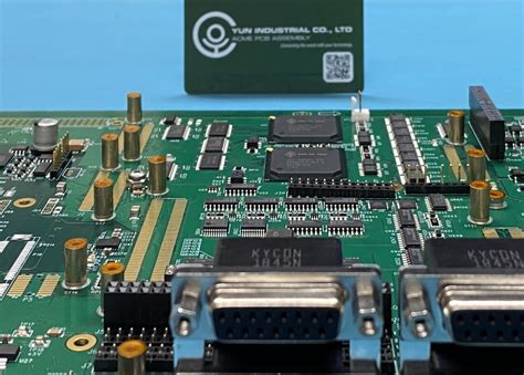
In the ever-evolving world of electronics, the demand for smaller, faster, and more efficient devices has driven the development of advanced printed circuit board (PCB) technologies. Among these, High-Density Interconnect (HDI) multilayer PCBs have emerged as a cornerstone in the design and manufacture of modern electronic devices. HDI PCBs are characterized by their high wiring density, which allows for more complex circuitry in a smaller footprint. This article delves into the intricacies of HDI multilayer PCBs, exploring their design, manufacturing processes, advantages, applications, and future trends.
1. Understanding HDI Multilayer PCBs
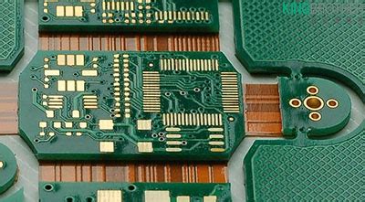
HDI multilayer PCBs are a type of PCB that incorporates high-density interconnect technology to achieve finer lines and spaces, smaller vias, and higher connection pad density than conventional PCBs. These boards typically feature multiple layers of conductive material separated by insulating layers, with intricate interconnections between them. The term “multilayer” refers to the presence of more than two conductive layers, which are laminated together to form a single PCB.
The key distinguishing feature of HDI PCBs is the use of microvias, which are small holes drilled into the PCB to create electrical connections between different layers. Microvias are significantly smaller than traditional through-hole vias, allowing for higher routing density and more compact designs. Additionally, HDI PCBs often employ advanced materials and manufacturing techniques to achieve the desired performance characteristics.
2. Design Considerations for HDI Multilayer PCBs
Designing an HDI multilayer PCB requires careful consideration of several factors to ensure optimal performance and manufacturability. Some of the key design considerations include:
2.1 Layer Stack-up
The layer stack-up is a critical aspect of HDI PCB design. It determines the number of conductive layers, the arrangement of signal and power planes, and the placement of microvias. A well-planned layer stack-up can minimize signal interference, reduce electromagnetic interference (EMI), and improve thermal management.
2.2 Microvia Technology
Microvias are a defining feature of HDI PCBs. They can be classified into several types, including blind vias, buried vias, and staggered or stacked vias. Blind vias connect an outer layer to one or more inner layers, while buried vias connect inner layers without reaching the outer layers. Stacked vias involve multiple microvias stacked on top of each other, allowing for connections across multiple layers. The choice of microvia technology depends on the specific design requirements and the complexity of the circuit.
2.3 Signal Integrity
Signal integrity is a crucial consideration in HDI PCB design, especially in high-speed applications. Factors such as impedance matching, crosstalk, and signal attenuation must be carefully managed to ensure reliable signal transmission. The use of controlled impedance traces, differential pairs, and proper grounding techniques can help maintain signal integrity.
2.4 Thermal Management
HDI PCBs often operate in high-power or high-density environments, making thermal management a critical design consideration. Effective thermal management techniques, such as the use of thermal vias, heat sinks, and thermally conductive materials, can help dissipate heat and prevent overheating.
2.5 Manufacturability
Designing for manufacturability is essential to ensure that the HDI PCB can be produced efficiently and cost-effectively. This involves considering factors such as material selection, minimum feature sizes, and the capabilities of the manufacturing process. Collaboration between designers and manufacturers is crucial to address potential manufacturing challenges early in the design process.

3. Manufacturing Processes for HDI Multilayer PCBs
The manufacturing of HDI multilayer PCBs involves several advanced processes that differ from those used in conventional PCB fabrication. Some of the key manufacturing steps include:
3.1 Material Selection
The choice of materials is critical in HDI PCB manufacturing. High-performance materials, such as low-loss laminates and high-temperature substrates, are often used to meet the demanding requirements of HDI designs. These materials offer superior electrical, thermal, and mechanical properties, enabling the production of high-quality HDI PCBs.
3.2 Laser Drilling
Laser drilling is the primary method used to create microvias in HDI PCBs. This process involves using a high-precision laser to drill small holes in the PCB substrate. Laser drilling allows for the creation of microvias with diameters as small as 50 microns, enabling high-density interconnections.
3.3 Sequential Lamination
Sequential lamination is a process used to build up the layers of an HDI PCB. This involves laminating multiple layers of conductive and insulating materials together, with microvias drilled and plated between each layer. The process is repeated until the desired number of layers is achieved. Sequential lamination allows for the creation of complex multilayer structures with high-density interconnections.
3.4 Copper Plating
Copper plating is used to create the conductive traces and vias in the PCB. In HDI PCBs, electroplating is commonly used to deposit copper into the microvias and onto the surface of the substrate. The plating process must be carefully controlled to ensure uniform copper deposition and reliable electrical connections.
3.5 Surface Finish
The surface finish is applied to the exposed copper surfaces of the PCB to protect them from oxidation and improve solderability. Common surface finishes for HDI PCBs include electroless nickel immersion gold (ENIG), immersion silver, and organic solderability preservatives (OSP). The choice of surface finish depends on the specific application and performance requirements.
3.6 Electrical Testing
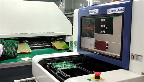
Electrical testing is a critical step in the manufacturing process to ensure the functionality and reliability of the HDI PCB. Automated optical inspection (AOI), electrical continuity testing, and impedance testing are commonly used to verify the integrity of the PCB. Any defects or issues identified during testing must be addressed before the PCB is shipped to the customer.
4. Advantages of HDI Multilayer PCBs
HDI multilayer PCBs offer several advantages over conventional PCBs, making them ideal for a wide range of applications. Some of the key advantages include:
4.1 Increased Circuit Density
The primary advantage of HDI PCBs is their ability to accommodate a higher density of circuits in a smaller footprint. This is achieved through the use of microvias, finer traces, and tighter spacing between components. The increased circuit density allows for more complex and sophisticated designs, enabling the development of advanced electronic devices.
4.2 Improved Signal Integrity
HDI PCBs are designed to minimize signal loss and interference, making them well-suited for high-speed and high-frequency applications. The use of controlled impedance traces, differential pairs, and advanced materials helps maintain signal integrity, ensuring reliable performance in demanding environments.
4.3 Enhanced Thermal Management
The compact design of HDI PCBs, combined with advanced thermal management techniques, allows for efficient heat dissipation. This is particularly important in high-power applications, where overheating can lead to performance degradation or failure. Effective thermal management helps ensure the long-term reliability of the PCB.
4.4 Reduced Size and Weight
The high-density interconnections and compact design of HDI PCBs enable the production of smaller and lighter electronic devices. This is particularly beneficial in applications where space and weight are critical factors, such as in portable electronics, aerospace, and automotive systems.
4.5 Cost-Effectiveness
While the initial design and manufacturing costs of HDI PCBs may be higher than those of conventional PCBs, the overall cost-effectiveness is often improved. The reduced size and weight of HDI PCBs can lead to savings in materials, shipping, and assembly costs. Additionally, the improved performance and reliability of HDI PCBs can result in lower maintenance and replacement costs over the lifetime of the product.

5. Applications of HDI Multilayer PCBs
HDI multilayer PCBs are used in a wide range of applications across various industries. Some of the key applications include:
5.1 Consumer Electronics
HDI PCBs are widely used in consumer electronics, such as smartphones, tablets, laptops, and wearable devices. The compact design and high circuit density of HDI PCBs enable the development of smaller, lighter, and more powerful devices with advanced features.
5.2 Telecommunications
The telecommunications industry relies on HDI PCBs for the production of high-speed and high-frequency communication equipment, such as routers, switches, and base stations. The improved signal integrity and thermal management of HDI PCBs are essential for ensuring reliable performance in these applications.
5.3 Automotive Electronics
The automotive industry is increasingly adopting HDI PCBs for use in advanced driver-assistance systems (ADAS), infotainment systems, and engine control units (ECUs). The compact design and high reliability of HDI PCBs make them well-suited for the demanding environments of modern vehicles.
5.4 Medical Devices
HDI PCBs are used in a variety of medical devices, including imaging systems, diagnostic equipment, and implantable devices. The high circuit density and reliability of HDI PCBs are critical for ensuring the performance and safety of these devices.
5.5 Aerospace and Defense
The aerospace and defense industries require high-performance PCBs that can withstand extreme conditions and provide reliable operation. HDI PCBs are used in applications such as avionics, radar systems, and satellite communications, where their compact design and high reliability are essential.
6. Future Trends in HDI Multilayer PCBs
As the demand for smaller, faster, and more efficient electronic devices continues to grow, the development of HDI multilayer PCBs is expected to advance further. Some of the key trends shaping the future of HDI PCBs include:
6.1 Increased Use of Advanced Materials
The development of new materials with superior electrical, thermal, and mechanical properties is expected to drive the evolution of HDI PCBs. Materials such as low-loss laminates, high-temperature substrates, and flexible substrates are likely to see increased adoption in HDI designs.
6.2 Adoption of Additive Manufacturing
Additive manufacturing, or 3D printing, is emerging as a promising technology for PCB fabrication. This technology has the potential to revolutionize the production of HDI PCBs by enabling the creation of complex, high-density interconnections with greater precision and efficiency.
6.3 Integration of Embedded Components
The integration of embedded components, such as resistors, capacitors, and inductors, directly into the PCB substrate is expected to become more prevalent in HDI designs. This approach can further reduce the size and weight of electronic devices while improving performance and reliability.
6.4 Development of Ultra-HDI PCBs
Ultra-HDI PCBs, which feature even finer lines and spaces, smaller vias, and higher connection pad densities than traditional HDI PCBs, are expected to gain traction in the coming years. These PCBs will enable the development of even more compact and sophisticated electronic devices.
6.5 Focus on Sustainability
As environmental concerns continue to grow, there is an increasing focus on sustainability in the electronics industry. The development of eco-friendly materials, manufacturing processes, and recycling methods for HDI PCBs is expected to become a key area of research and innovation.

Conclusion
HDI multilayer PCBs have revolutionized the electronics industry by enabling the development of smaller, faster, and more efficient devices. Their high circuit density, improved signal integrity, and enhanced thermal management make them ideal for a wide range of applications, from consumer electronics to aerospace and defense. As technology continues to advance, the future of HDI PCBs looks promising, with trends such as the adoption of advanced materials, additive manufacturing, and embedded components driving further innovation. By staying at the forefront of these developments, manufacturers and designers can continue to push the boundaries of what is possible in modern electronics.


