High-Density Interconnect (HDI) PCB Manufacturing: Revolutionizing Modern Electronics
Introduction
In the rapidly evolving world of electronics, the demand for smaller, faster, and more efficient devices has never been greater. High-Density Interconnect (HDI) Printed Circuit Boards (PCBs) have emerged as a critical technology to meet these demands. HDI PCBs are at the heart of modern electronics, enabling the development of compact, high-performance devices such as smartphones, tablets, wearable technology, and advanced medical equipment. This article explores the intricacies of HDI PCB manufacturing, its benefits, applications, and the future of this transformative technology.
What is HDI PCB?
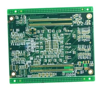
HDI PCBs are a type of printed circuit board characterized by their high wiring density per unit area. They feature finer lines and spaces, smaller vias, and higher connection pad density than conventional PCBs. The key distinguishing feature of HDI PCBs is the use of microvias, which are tiny holes drilled into the board to create connections between different layers. These microvias allow for more complex and compact designs, making HDI PCBs ideal for modern electronic devices that require high performance in a small form factor.
The Manufacturing Process of HDI PCBs
The manufacturing process of HDI PCBs is more complex and precise than that of traditional PCBs. It involves several advanced techniques and technologies to achieve the high density and precision required. Below is an overview of the key steps in HDI PCB manufacturing:
- Design and Layout
The process begins with the design and layout of the PCB. Engineers use specialized software to create a detailed blueprint of the board, including the placement of components, routing of traces, and the location of microvias. The design must account for signal integrity, thermal management, and manufacturability. - Material Selection
HDI PCBs require high-quality materials to ensure reliability and performance. Common materials include high-performance laminates, copper foils, and solder masks. The choice of materials depends on the specific application and performance requirements. - Layup and Lamination
HDI PCBs typically consist of multiple layers of conductive and insulating materials. The layers are carefully aligned and laminated together under high pressure and temperature to form a solid board. The use of sequential lamination processes allows for the creation of complex multilayer structures with microvias. - Drilling and Microvia Formation
One of the most critical steps in HDI PCB manufacturing is the creation of microvias. These tiny holes are drilled using laser drilling technology, which offers the precision required for high-density designs. The microvias are then plated with copper to create electrical connections between layers. - Pattern Plating and Etching
After drilling, the board undergoes pattern plating and etching to create the conductive traces and pads. This process involves applying a thin layer of copper to the surface of the board and then using photolithography to define the desired circuit pattern. The excess copper is then etched away, leaving behind the intricate network of traces. - Solder Mask Application
A solder mask is applied to the board to protect the copper traces and prevent short circuits. The solder mask also provides insulation and improves the durability of the board. The mask is typically applied using a screen printing or photoimaging process. - Surface Finish
The final step in the manufacturing process is the application of a surface finish to the exposed copper areas. Common surface finishes include HASL (Hot Air Solder Leveling), ENIG (Electroless Nickel Immersion Gold), and OSP (Organic Solderability Preservative). The surface finish enhances solderability and protects the copper from oxidation. - Testing and Inspection
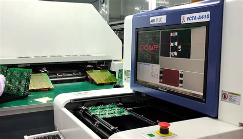
Quality control is a critical aspect of HDI PCB manufacturing. The finished boards undergo rigorous testing and inspection to ensure they meet the required specifications and performance standards. This includes electrical testing, visual inspection, and automated optical inspection (AOI) to detect any defects or inconsistencies.
Benefits of HDI PCBs
HDI PCBs offer numerous advantages over traditional PCBs, making them the preferred choice for many modern electronic applications. Some of the key benefits include:
- Increased Circuit Density
HDI PCBs allow for a higher density of components and connections, enabling the design of smaller and more compact devices. This is particularly important for portable electronics, where space is at a premium. - Improved Signal Integrity
The use of microvias and finer traces reduces signal loss and improves signal integrity. This is crucial for high-speed and high-frequency applications, where maintaining signal quality is essential. - Enhanced Thermal Management
HDI PCBs can be designed with advanced thermal management features, such as thermal vias and heat sinks, to dissipate heat more effectively. This helps to prevent overheating and ensures the reliability of the device. - Reduced Weight and Size
The compact design of HDI PCBs reduces the overall weight and size of electronic devices. This is particularly beneficial for applications such as aerospace and automotive, where weight reduction is critical. - Higher Reliability
The advanced manufacturing techniques used in HDI PCB production result in higher reliability and durability. The use of microvias and sequential lamination processes reduces the risk of defects and improves the overall quality of the board. - Cost Efficiency
While the initial cost of HDI PCBs may be higher than traditional PCBs, the overall cost efficiency is often better. The reduced size and weight of the boards can lead to savings in materials, shipping, and assembly costs. Additionally, the improved performance and reliability can reduce the need for costly repairs and replacements.
Applications of HDI PCBs
HDI PCBs are used in a wide range of industries and applications, thanks to their ability to deliver high performance in a compact form factor. Some of the most common applications include:
- Consumer Electronics
HDI PCBs are widely used in consumer electronics, such as smartphones, tablets, laptops, and wearable devices. The demand for smaller, lighter, and more powerful devices has driven the adoption of HDI technology in this sector. - Medical Devices
The medical industry relies on HDI PCBs for the development of advanced medical devices, such as imaging equipment, diagnostic tools, and implantable devices. The high density and reliability of HDI PCBs are essential for these critical applications. - Automotive Electronics
The automotive industry is increasingly adopting HDI PCBs for use in advanced driver-assistance systems (ADAS), infotainment systems, and electric vehicle (EV) components. The compact design and high reliability of HDI PCBs make them ideal for the demanding conditions of automotive applications. - Aerospace and Defense
HDI PCBs are used in aerospace and defense applications, where reliability and performance are paramount. They are used in avionics, communication systems, and military equipment, where space and weight constraints are critical. - Industrial Equipment
HDI PCBs are also used in industrial equipment, such as automation systems, robotics, and control systems. The high density and reliability of HDI PCBs enable the development of more efficient and compact industrial solutions.
The Future of HDI PCB Manufacturing
As the demand for smaller, faster, and more efficient electronic devices continues to grow, the importance of HDI PCB manufacturing will only increase. Several trends are shaping the future of HDI PCB technology:
- Miniaturization
The trend towards miniaturization is expected to continue, with HDI PCBs playing a key role in enabling the development of even smaller and more compact devices. Advances in materials and manufacturing techniques will further enhance the capabilities of HDI PCBs. - Higher Speeds and Frequencies
As electronic devices become more advanced, the need for higher speeds and frequencies will drive the development of HDI PCBs with improved signal integrity and reduced signal loss. This will be particularly important for applications such as 5G communication and high-performance computing. - Increased Integration
The integration of more functions and components into a single PCB will continue to be a key trend. HDI PCBs will enable the development of more complex and multifunctional devices, reducing the need for multiple boards and connectors. - Sustainability
The electronics industry is increasingly focused on sustainability, and HDI PCB manufacturing is no exception. The use of environmentally friendly materials and processes, as well as the development of recyclable and biodegradable PCBs, will be important areas of focus in the future. - Advanced Manufacturing Techniques
Advances in manufacturing techniques, such as additive manufacturing (3D printing) and artificial intelligence (AI), will further enhance the capabilities of HDI PCB production. These technologies will enable more precise and efficient manufacturing processes, reducing costs and improving quality.
Conclusion
HDI PCB manufacturing is a critical technology that is driving the development of modern electronics. The ability to create high-density, high-performance PCBs in a compact form factor has enabled the development of smaller, faster, and more efficient devices across a wide range of industries. As the demand for advanced electronic devices continues to grow, the importance of HDI PCB manufacturing will only increase. With ongoing advancements in materials, manufacturing techniques, and design capabilities, the future of HDI PCB technology is bright, promising even greater innovation and performance in the years to come.


