High-Density Interconnect (HDI) PCB Prototyping: Revolutionizing Modern Electronics
Introduction
In the ever-evolving world of electronics, the demand for smaller, faster, and more efficient devices has driven the need for advanced printed circuit board (PCB) technologies. High-Density Interconnect (HDI) PCBs have emerged as a critical enabler of this trend, offering superior performance, reduced size, and enhanced functionality compared to traditional PCBs. HDI PCB prototyping plays a pivotal role in the development of cutting-edge electronic devices, allowing engineers to test and refine designs before mass production. This article explores the fundamentals of HDI PCBs, the prototyping process, their advantages, applications, and future trends.
What is HDI PCB?
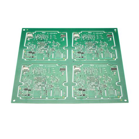
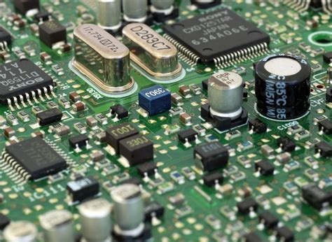
HDI PCBs are a type of printed circuit board characterized by their high wiring density per unit area. They achieve this through the use of finer lines and spaces, smaller vias, and higher connection pad density. Key features of HDI PCBs include:
- Microvias: These are small holes drilled using laser technology, enabling connections between layers in a compact space.
- Fine Pitch Components: HDI PCBs support components with very small pin spacing, allowing for more complex designs.
- Multiple Layers: HDI boards often incorporate multiple layers, including buried and blind vias, to maximize space utilization.
- Advanced Materials: High-performance materials with improved thermal and electrical properties are used to meet the demands of high-speed and high-frequency applications.
HDI PCBs are essential for modern electronics, where space constraints and performance requirements are critical.
The HDI PCB Prototyping Process
Prototyping is a crucial step in the development of HDI PCBs. It allows designers to validate their concepts, identify potential issues, and optimize the design before moving to full-scale production. The HDI PCB prototyping process typically involves the following steps:
- Design and Layout:
- Engineers use specialized software to create the PCB layout, considering factors such as signal integrity, thermal management, and manufacturability.
- The design includes microvias, blind vias, and buried vias to achieve the desired density and functionality.
- Material Selection:
- The choice of materials is critical for HDI PCBs. High-performance substrates, such as FR-4, polyimide, or ceramic-filled materials, are selected based on the application’s requirements.
- Laser Drilling:
- Microvias are created using laser drilling technology, which offers precision and consistency. This step is essential for achieving the high-density interconnects that define HDI PCBs.
- Plating and Etching:
- The drilled vias are plated with copper to establish electrical connections between layers.
- The copper layers are then etched to create the desired circuit patterns.
- Lamination:
- Multiple layers of the PCB are laminated together under high pressure and temperature to form a solid board.
- Testing and Validation:
- Prototypes undergo rigorous testing to ensure they meet design specifications and performance criteria.
- Tests may include electrical continuity checks, signal integrity analysis, and thermal performance evaluation.
- Iterative Refinement:
- Based on test results, designers may refine the prototype to address any issues or improve performance.
Advantages of HDI PCB Prototyping
HDI PCB prototyping offers numerous benefits, making it an indispensable part of modern electronics development:
- Compact Design:
- HDI technology enables the creation of smaller PCBs with higher functionality, ideal for portable and wearable devices.
- Improved Performance:
- The reduced distance between components and shorter signal paths result in faster signal transmission and reduced signal loss.
- Enhanced Reliability:
- Advanced manufacturing techniques and materials improve the durability and reliability of HDI PCBs.
- Cost Efficiency:
- While HDI PCBs may have higher initial costs, their compact design and improved performance can lead to overall cost savings in the final product.
- Faster Time-to-Market:
- Prototyping allows for rapid iteration and validation, accelerating the development process.
Applications of HDI PCB Prototypes
HDI PCB prototypes are used in a wide range of industries and applications, including:
- Consumer Electronics:
- Smartphones, tablets, and laptops rely on HDI PCBs for their compact size and high performance.
- Medical Devices:
- Medical equipment, such as imaging systems and implantable devices, benefit from the reliability and miniaturization offered by HDI technology.
- Automotive Electronics:
- Advanced driver-assistance systems (ADAS) and infotainment systems require HDI PCBs for their complex functionality and durability.
- Aerospace and Defense:
- HDI PCBs are used in avionics, satellites, and military equipment, where performance and reliability are critical.
- Internet of Things (IoT):
- IoT devices, such as smart home sensors and industrial automation systems, leverage HDI PCBs for their compact design and low power consumption.
Challenges in HDI PCB Prototyping
Despite its many advantages, HDI PCB prototyping presents several challenges:
- Complex Design:
- The intricate layout and high density of HDI PCBs require advanced design tools and expertise.
- Manufacturing Precision:
- Achieving the fine features and tight tolerances of HDI PCBs demands state-of-the-art equipment and processes.
- Cost:
- The advanced materials and technologies used in HDI PCBs can result in higher prototyping costs compared to traditional PCBs.
- Testing Complexity:
- The high density and complexity of HDI PCBs make testing and validation more challenging.
Future Trends in HDI PCB Prototypin
As technology continues to advance, several trends are shaping the future of HDI PCB prototyping:
- Increased Miniaturization:
- The demand for even smaller and more powerful devices will drive further advancements in HDI technology.
- Advanced Materials:
- The development of new materials with enhanced thermal, electrical, and mechanical properties will enable higher performance and reliability.
- 3D Printing:
- Additive manufacturing techniques, such as 3D printing, may revolutionize PCB prototyping by enabling rapid and flexible production.
- AI and Automation:
- Artificial intelligence and automation will play a growing role in optimizing the design and manufacturing processes for HDI PCBs.
- Sustainability:
- The industry is increasingly focusing on eco-friendly materials and processes to reduce the environmental impact of PCB manufacturing.
Conclusion
HDI PCB prototyping is at the forefront of modern electronics development, enabling the creation of smaller, faster, and more efficient devices. By leveraging advanced technologies and materials, HDI PCBs meet the demands of a wide range of applications, from consumer electronics to aerospace. While challenges remain, ongoing advancements in design tools, manufacturing processes, and materials promise to further enhance the capabilities of HDI PCBs. As the electronics industry continues to evolve, HDI PCB prototyping will remain a critical enabler of innovation, driving the development of next-generation technologies.


