High Density Interconnect (HDI) PCB: Revolutionizing Modern Electronics
Introduction to HDI PCB Technology
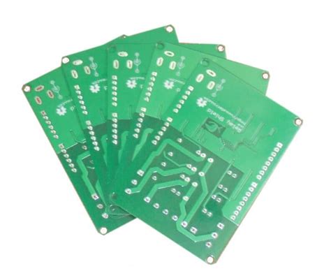
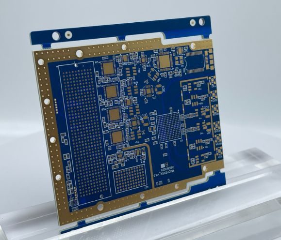
High Density Interconnect (HDI) printed circuit boards represent one of the most significant advancements in PCB technology in recent decades. As electronic devices continue to shrink in size while increasing in functionality, HDI PCBs have emerged as the solution to accommodate these competing demands. These advanced circuit boards enable higher wiring density per unit area through finer lines and spaces, smaller vias, and higher connection pad density compared to conventional PCBs.
The development of HDI technology has been driven by the relentless miniaturization of electronic devices across industries—from smartphones and wearables to medical devices and aerospace systems. As consumers demand more powerful yet compact devices, manufacturers have turned to HDI PCBs to pack more functionality into smaller form factors without compromising performance or reliability.
Key Characteristics of HDI PCBs
HDI PCBs distinguish themselves from traditional printed circuit boards through several defining characteristics:
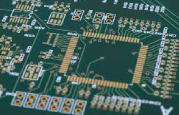
Microvias: Perhaps the most distinctive feature of HDI boards, microvias are small laser-drilled holes typically less than 150 microns in diameter. These allow for connections between layers in the PCB stackup with minimal space consumption. Microvias can be blind (connecting an outer layer to one or more inner layers) or buried (connecting only inner layers).
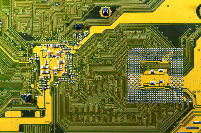
Fine Line Geometry: HDI PCBs utilize much finer trace widths and spacing than conventional boards, often with lines and spaces measuring 3 mils (75 microns) or less. This enables more circuitry to be routed in the same or smaller area.
High Layer Count: While not all HDI boards have high layer counts, the technology enables more layers to be effectively utilized in a given thickness due to the use of thin dielectric materials and microvias.
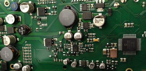
Advanced Materials: HDI PCBs often employ specialized materials with improved electrical properties, thermal stability, and dimensional stability to support the fine features and high reliability requirements.
Sequential Lamination: Many HDI designs require multiple lamination cycles to build up the layer structure with embedded microvias, distinguishing them from standard multilayer boards that typically use a single lamination process.
HDI PCB Design Considerations
Designing an HDI printed circuit board requires careful consideration of several factors that differ from conventional PCB design:
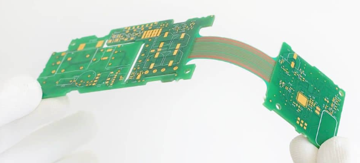
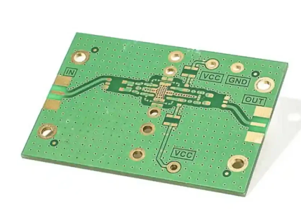
Stackup Planning: The layer stackup must be meticulously planned to optimize signal integrity, power distribution, and thermal management while accommodating the via structures. Designers must decide between various HDI architectures like 1+N+1, 2+N+2, or more complex sequential build-up structures.
Via Selection: HDI designs may incorporate various via types including through-hole vias, blind/buried vias, and microvias. The selection and placement of these vias significantly impact routing density and signal performance.
Routing Strategies: With finer pitch components and high pin counts, HDI routing requires advanced strategies such as escape routing, fan-out patterns, and appropriate use of via-in-pad techniques.
Signal Integrity: High-speed signals in dense environments require careful attention to impedance control, crosstalk mitigation, and proper return paths. The compact nature of HDI can both help (shorter paths) and challenge (tighter coupling) signal integrity.
Thermal Management: Increased component density leads to higher power densities, necessitating thoughtful thermal design including proper via placement for heat dissipation and potential incorporation of thermal vias.
Manufacturing Constraints: Design rules must account for the capabilities and limitations of HDI manufacturing processes to ensure producibility and yield.
Manufacturing Processes for HDI PCBs
The production of HDI printed circuit boards involves specialized processes that go beyond conventional PCB fabrication:
Laser Drilling: Microvias are typically created using precision laser drilling systems capable of creating holes as small as 25-50 microns in diameter. Common lasers include CO₂ and UV lasers, each with advantages for different materials.
Sequential Lamination: Complex HDI boards may require multiple lamination cycles where layers are built up sequentially with dielectric and copper layers, with microvias connecting between adjacent layers.
Advanced Plating: Microvia plating presents challenges due to the high aspect ratios (depth to diameter) of these small features. Specialized plating processes ensure complete via filling or conformal plating for reliable interconnects.
Fine Line Imaging: Achieving the ultra-fine traces in HDI boards requires advanced photolithography processes, often using direct imaging systems that project the circuit pattern directly onto the photoresist-coated panel without phototools.
Materials Handling: The thin, delicate materials used in HDI manufacturing require careful handling throughout the fabrication process to prevent damage or deformation.
Inspection and Testing: HDI boards demand more rigorous inspection, often employing automated optical inspection (AOI), X-ray inspection for via integrity, and specialized electrical testing to verify the dense interconnects.
Applications of HDI PCB Technology
HDI printed circuit boards have become essential components across numerous industries where miniaturization and high performance are critical:
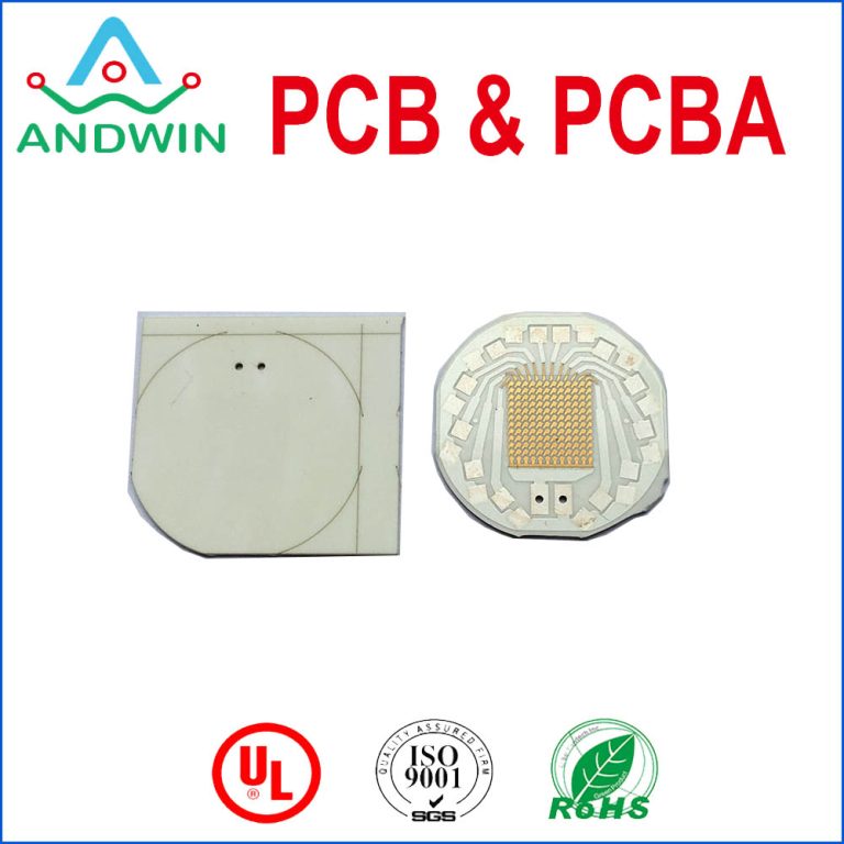
Consumer Electronics: Smartphones, tablets, and wearables were among the first and remain the most widespread applications of HDI technology. The compact form factors and high functionality of these devices rely heavily on HDI PCBs.
Medical Devices: From implantable devices to advanced imaging equipment, medical technology benefits from HDI’s ability to pack sophisticated electronics into small, reliable packages.
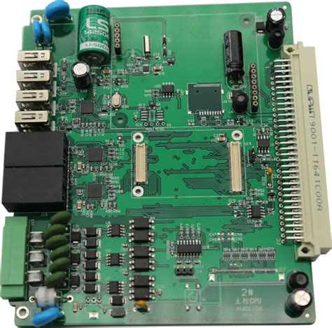
Automotive Electronics: Modern vehicles incorporate numerous electronic systems for infotainment, advanced driver assistance systems (ADAS), and vehicle control, many of which utilize HDI technology.
Aerospace and Defense: Avionics, communications equipment, and guidance systems employ HDI PCBs for their reliability and high-density capabilities in constrained spaces.
Networking and Telecommunications: High-speed networking equipment, routers, and switches benefit from HDI’s ability to handle high-frequency signals in compact designs.
Internet of Things (IoT): The proliferation of connected devices across industries drives demand for small, powerful PCBs that can support wireless connectivity and sensor integration.
Advantages of HDI PCB Technology
The adoption of HDI technology offers numerous benefits for electronic products and systems:
Space Reduction: HDI PCBs can reduce board area requirements by 50% or more compared to conventional designs for equivalent functionality, enabling smaller end products.
Improved Electrical Performance: Shorter signal paths reduce propagation delays and signal loss, while proper HDI design can enhance signal integrity for high-speed applications.
Enhanced Reliability: The microvia structure in HDI boards often proves more reliable than through-hole vias for thermal cycling, as the smaller via size experiences less thermal stress.
Design Flexibility: HDI technology allows for more creative packaging solutions and integration of complex components that wouldn’t be feasible with traditional PCB approaches.
Weight Reduction: The compact nature of HDI designs, combined with potential reductions in layer count for equivalent functionality, can significantly decrease board weight—critical for portable and aerospace applications.
Cost Optimization: While HDI PCBs have higher unit costs, the overall system cost may be lower due to reduced layer counts, smaller form factors, and improved yields in assembly.
Challenges in HDI PCB Implementation
Despite its advantages, HDI technology presents several challenges that designers and manufacturers must address:
Higher Fabrication Costs: The specialized materials, equipment, and processes required for HDI manufacturing result in higher costs compared to conventional PCBs, though this gap is narrowing as the technology matures.
Design Complexity: HDI layouts require more sophisticated design techniques and careful planning, often necessitating specialized expertise and advanced EDA tools.
Thermal Management: The high component density in HDI designs can create localized hot spots that require careful thermal analysis and mitigation strategies.
Signal Integrity Issues: The tight spacing in HDI boards can lead to increased crosstalk and electromagnetic interference if not properly managed through careful design.
Manufacturing Yield: The fine features and complex structures in HDI PCBs can impact production yields, particularly for new designs or when pushing the limits of the technology.
Testing Difficulties: The high density of interconnects makes electrical testing more challenging, requiring advanced test equipment and methodologies.
Future Trends in HDI PCB Technology
The evolution of HDI technology continues as demands for miniaturization and performance intensify:
Ultra HDI: The next generation of HDI pushes feature sizes even smaller, with lines/spaces below 2 mils (50 microns) and microvias approaching 25 microns in diameter.
Embedded Components: Passive components (resistors, capacitors) and even some active components are being embedded within the PCB layers to save surface space and improve performance.
Advanced Materials: New dielectric materials with better high-frequency characteristics, thermal properties, and dimensional stability are enabling further HDI advancements.
3D Packaging: HDI technology is converging with 3D packaging approaches like package-on-package (PoP) and system-in-package (SiP) for even greater integration.
Additive Manufacturing: Semi-additive and fully additive processes are being developed to create finer features more reliably than traditional subtractive methods.
Optical Interconnects: Some advanced HDI designs are beginning to incorporate optical waveguides alongside electrical traces for high-speed data transmission.
Conclusion
High Density Interconnect PCB technology has revolutionized electronic product design, enabling the compact, powerful devices we rely on daily. As the technology continues to advance, HDI will play an increasingly critical role in meeting the demands of next-generation electronics across industries. While challenges remain in design, manufacturing, and testing, ongoing innovations in materials, processes, and design methodologies are steadily overcoming these barriers.
For engineers and product developers, understanding HDI technology and its capabilities is no longer optional but essential for creating competitive electronic products. As we look to the future, HDI PCBs will likely form the foundation for emerging technologies like flexible hybrid electronics, advanced IoT devices, and next-generation computing systems, continuing their transformative impact on the electronics industry.