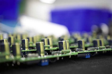
High frequency pcb
Design Considerations for High Frequency PCBs
When designing high frequency printed circuit boards (PCBs), several critical considerations must be taken into account to ensure optimal performance and reliability. High frequency PCBs are integral to applications such as telecommunications, radar systems, and advanced computing, where signal integrity and minimal loss are paramount. As frequencies increase, the challenges associated with PCB design become more pronounced, necessitating a comprehensive understanding of the factors that influence performance.
One of the primary considerations in high frequency PCB design is the choice of materials.
The dielectric material used in the PCB substrate significantly affects signal propagation. Materials with low dielectric constant (Dk) and low dissipation factor (Df) are preferred, as they minimize signal loss and ensure faster signal transmission. Common materials include PTFE (polytetrafluoroethylene) and ceramic-filled laminates, which offer excellent electrical properties. However, these materials can be more expensive and challenging to work with compared to standard FR-4 substrates.
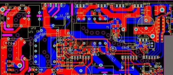
In addition to material selection, the layout of the PCB plays a crucial role in high frequency applications.
The layout must be meticulously planned to reduce electromagnetic interference (EMI) and crosstalk between traces. To achieve this, designers often employ techniques such as controlled impedance routing, where the width and spacing of traces are carefully calculated to maintain consistent impedance. This is particularly important for differential pairs, which are used to transmit high-speed signals with minimal interference.
Moreover, the use of ground planes is essential in high frequency PCB design.
Ground planes provide a return path for signals and help to reduce EMI by acting as a shield. They also contribute to the overall stability of the PCB by minimizing voltage fluctuations. It is advisable to use multiple ground planes in multilayer PCBs to further enhance signal integrity. Additionally, ensuring that vias, which connect different layers of the PCB, are properly designed is crucial. Vias can introduce inductance and capacitance, which may degrade signal quality if not managed correctly.
Thermal management is another important aspect to consider in high frequency PCB design.
High frequency components often generate significant heat, which can affect performance and reliability if not adequately dissipated. Designers must incorporate thermal vias, heat sinks, and appropriate trace widths to manage heat effectively. The choice of materials also impacts thermal performance, as some substrates offer better thermal conductivity than others.
Furthermore, the integration of simulation tools in the design process can greatly enhance the accuracy and efficiency of high frequency PCB design.
Simulation software allows designers to model the electrical behavior of the PCB and identify potential issues before physical prototyping. This can save time and resources by reducing the need for multiple iterations.
Finally, manufacturing tolerances must be considered during the design phase. High frequency PCBs often require tighter tolerances than standard PCBs to ensure that the physical dimensions align with the electrical specifications. Collaborating closely with manufacturers can help designers understand the limitations and capabilities of the fabrication process, leading to more successful outcomes.
In conclusion, designing high frequency PCBs involves a complex interplay of material selection, layout optimization, thermal management, and manufacturing considerations. By addressing these factors with precision and foresight, designers can create PCBs that meet the demanding requirements of high frequency applications, ensuring robust performance and reliability in advanced technological environments.

Material Selection for High Frequency PCB Applications
In the realm of high-frequency printed circuit boards (PCBs), material selection plays a pivotal role in determining the performance and reliability of the final product. As electronic devices continue to evolve, demanding faster speeds and higher frequencies, the need for specialized materials becomes increasingly critical. High-frequency PCBs are typically used in applications such as telecommunications, radar systems, and advanced computing, where signal integrity and minimal loss are paramount. Therefore, understanding the properties and implications of various materials is essential for engineers and designers working in this field.
To begin with, one of the primary considerations in material selection for high-frequency PCBs is the dielectric constant (Dk).
The dielectric constant affects the speed at which an electrical signal can travel through the material. Materials with a lower dielectric constant are generally preferred for high-frequency applications because they allow signals to propagate faster and with less distortion. Common materials used in these applications include PTFE (polytetrafluoroethylene), ceramic-filled laminates, and hydrocarbon-based laminates. Each of these materials offers a unique set of properties that can be leveraged depending on the specific requirements of the application.
In addition to the dielectric constant, the dissipation factor (Df) is another critical parameter to consider.
The dissipation factor measures the energy loss as heat within the material, which can significantly impact the efficiency of high-frequency circuits. Materials with a low dissipation factor are ideal for minimizing signal loss and ensuring that the PCB operates efficiently. PTFE, for instance, is renowned for its low dissipation factor, making it a popular choice for high-frequency applications. However, it is important to note that while PTFE offers excellent electrical properties, it can be challenging to process and may require specialized manufacturing techniques.
Moreover, thermal management is a crucial aspect of high-frequency PCB design.
As frequencies increase, so does the potential for heat generation, which can adversely affect the performance and longevity of the PCB. Therefore, selecting materials with good thermal conductivity is essential to dissipate heat effectively. Ceramic-filled laminates, for example, provide enhanced thermal management capabilities, making them suitable for applications where heat dissipation is a concern.
Furthermore, the coefficient of thermal expansion (CTE) is another factor that cannot be overlooked.
The CTE measures how much a material expands or contracts with temperature changes. A mismatch in CTE between the PCB material and other components can lead to mechanical stress and potential failure. Therefore, selecting materials with a CTE that closely matches that of the components is vital to ensure the reliability of the PCB under varying thermal conditions.
In conclusion, the selection of materials for high-frequency PCB applications is a complex process that requires careful consideration of various factors, including the dielectric constant, dissipation factor, thermal management, and coefficient of thermal expansion. By understanding these properties and how they interact with the specific requirements of the application, engineers and designers can make informed decisions that enhance the performance and reliability of high-frequency PCBs. As technology continues to advance, the demand for high-performance materials will only grow, underscoring the importance of material selection in the development of cutting-edge electronic devices.
Challenges in Manufacturing High Frequency PCBs
The manufacturing of high frequency printed circuit boards (PCBs) presents a unique set of challenges that distinguish it from the production of standard PCBs. As electronic devices continue to evolve, the demand for high frequency PCBs has surged, driven by applications in telecommunications, aerospace, and advanced computing. These PCBs are essential for devices that operate at microwave frequencies, typically above 1 GHz, where signal integrity and performance are paramount. However, the complexities involved in their production require a deep understanding of materials, design, and fabrication processes.
One of the primary challenges in manufacturing high frequency PCBs is the selection of suitable materials.
Unlike standard PCBs, which often use FR-4 substrates, high frequency PCBs require materials with low dielectric constants and low loss tangents to minimize signal loss and ensure efficient transmission. Materials such as PTFE (polytetrafluoroethylene), ceramics, and specialized laminates are commonly used. However, these materials can be more expensive and difficult to handle, necessitating precise control over the manufacturing process to maintain consistency and quality.
In addition to material selection, the design of high frequency PCBs poses significant challenges.
The layout must be meticulously planned to minimize electromagnetic interference (EMI) and crosstalk between traces. This often involves the use of advanced simulation tools to predict and mitigate potential issues before fabrication. Furthermore, the miniaturization of components and the need for high-density interconnects add layers of complexity to the design process. Designers must carefully consider trace width, spacing, and the use of ground planes to ensure optimal performance.
The fabrication process itself introduces further challenges.
High frequency PCBs often require tighter tolerances and more precise manufacturing techniques than standard PCBs. For instance, the etching process must be carefully controlled to prevent over-etching, which can alter the impedance of the traces and degrade signal quality. Additionally, drilling vias in high frequency PCBs demands high precision to avoid defects that could impact performance. The use of laser drilling and other advanced techniques is often necessary to achieve the required accuracy.
Moreover, the assembly of high frequency PCBs can be particularly demanding.
The components used in these boards are often sensitive to heat, necessitating careful control of reflow soldering temperatures to prevent damage. The use of surface mount technology (SMT) is common, but it requires precise placement and soldering to ensure reliable connections. Any defects in assembly can lead to significant performance issues, making quality control a critical aspect of the manufacturing process.
Finally, testing and validation of high frequency PCBs are crucial to ensure they meet the stringent performance requirements.
This involves the use of specialized equipment to measure parameters such as insertion loss, return loss, and phase stability. The testing process can be time-consuming and requires skilled technicians to interpret the results accurately.
In conclusion, the manufacturing of high frequency PCBs is a complex and challenging endeavor that demands a high level of expertise and precision. From material selection and design to fabrication and testing, each step in the process must be carefully managed to produce boards that meet the demanding requirements of high frequency applications. As technology continues to advance, the ability to overcome these challenges will be essential for manufacturers seeking to remain competitive in this rapidly evolving field.
Testing and Validation Techniques for High Frequency PCBs
In the realm of modern electronics, high frequency printed circuit boards (PCBs) play a pivotal role in enabling the rapid transmission of signals across various devices. As the demand for faster and more efficient electronic systems continues to grow, the need for rigorous testing and validation techniques for high frequency PCBs becomes increasingly critical. These techniques ensure that the PCBs meet the stringent performance and reliability standards required in high-speed applications.
To begin with, one of the fundamental aspects of testing high frequency PCBs is impedance control.
Impedance, which is the resistance to the flow of alternating current, must be precisely managed to prevent signal distortion and loss. Manufacturers employ time domain reflectometry (TDR) to measure the impedance of the PCB traces. TDR sends a fast electrical pulse through the trace and measures the reflections caused by impedance mismatches. By analyzing these reflections, engineers can identify and rectify any discrepancies, ensuring that the PCB maintains the desired impedance levels.
In addition to impedance control, signal integrity testing is paramount for high frequency PCBs.
Signal integrity refers to the quality and reliability of the electrical signals as they travel through the PCB. Poor signal integrity can lead to data errors and system malfunctions. To assess signal integrity, engineers utilize eye diagram analysis, which provides a visual representation of a signal’s voltage over time. By examining the eye diagram, engineers can detect issues such as jitter, noise, and distortion, allowing them to make necessary adjustments to the PCB design or materials.
Moreover, electromagnetic compatibility (EMC) testing is essential to ensure that high frequency PCBs do not interfere with other electronic devices and comply with regulatory standards.
EMC testing involves evaluating the PCB’s emissions and susceptibility to electromagnetic interference (EMI). This is achieved through a series of tests, including radiated and conducted emissions tests, which measure the electromagnetic noise emitted by the PCB. Additionally, susceptibility tests assess the PCB’s ability to function correctly in the presence of external electromagnetic fields. By conducting thorough EMC testing, manufacturers can ensure that their high frequency PCBs operate harmoniously within their intended environments.
Thermal management is another critical consideration in the testing and validation of high frequency PCBs.
As these PCBs often operate at high speeds, they can generate significant amounts of heat, which can adversely affect performance and reliability. Thermal testing involves assessing the PCB’s ability to dissipate heat effectively. Techniques such as infrared thermography and thermal cycling tests are employed to evaluate the thermal performance of the PCB. These tests help identify potential hotspots and ensure that the PCB can maintain optimal operating temperatures under various conditions.
Finally, mechanical reliability testing is crucial to validate the durability of high frequency PCBs.
These tests simulate the physical stresses that the PCB may encounter during its lifecycle, such as vibration, shock, and flexing. By subjecting the PCB to these conditions, engineers can assess its mechanical robustness and identify any potential failure points. This ensures that the PCB can withstand the rigors of real-world applications without compromising its performance.
In conclusion, the testing and validation of high frequency PCBs involve a comprehensive suite of techniques designed to ensure their performance, reliability, and compliance with industry standards. By meticulously evaluating impedance control, signal integrity, electromagnetic compatibility, thermal management, and mechanical reliability, manufacturers can deliver high frequency PCBs that meet the demands of modern electronic systems. As technology continues to advance, these testing and validation techniques will remain indispensable in the development of cutting-edge electronic devices.