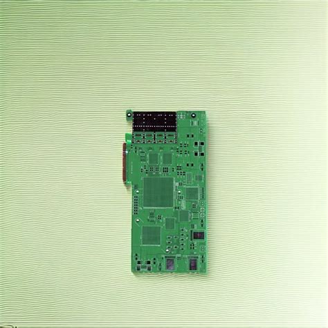
High frequency pcb board
Design Techniques For High Frequency PCB Boards
Designing high-frequency PCB boards requires a meticulous approach, as these boards are integral to the performance of modern electronic devices. The complexity of high-frequency circuits necessitates a deep understanding of electromagnetic theory, signal integrity, and thermal management.
To begin with, selecting the appropriate materials is crucial.
High-frequency PCBs often utilize materials such as PTFE (Teflon) or ceramic-filled laminates, which offer low dielectric constants and minimal signal loss. These materials help maintain signal integrity by reducing dielectric losses and ensuring consistent impedance throughout the board.
Transitioning to the layout design, it is essential to consider the trace geometry.
The width, spacing, and thickness of traces must be carefully calculated to match the characteristic impedance required by the circuit. Microstrip and stripline configurations are commonly used in high-frequency designs, as they provide controlled impedance paths. Additionally, maintaining a uniform trace width and avoiding sharp bends can minimize signal reflections and losses. The use of ground planes is another critical aspect, as they provide a return path for signals and help reduce electromagnetic interference (EMI). Ensuring a continuous ground plane beneath high-frequency traces can significantly enhance signal integrity.
Moreover, the placement of components plays a pivotal role in high-frequency PCB design.
Components should be positioned to minimize the length of high-frequency signal paths, thereby reducing potential signal degradation. Grouping components with similar functions can also help in minimizing crosstalk and EMI. Furthermore, decoupling capacitors should be placed as close as possible to power pins to filter out high-frequency noise effectively. The strategic placement of vias is equally important, as they can introduce inductance and affect signal integrity. Minimizing the number of vias in high-frequency paths and using blind or buried vias can mitigate these issues.
Thermal management is another critical consideration in high-frequency PCB design.
High-frequency circuits often generate significant heat, which can affect performance and reliability. Implementing thermal vias, heat sinks, and thermal pads can help dissipate heat efficiently. Additionally, selecting materials with high thermal conductivity can further enhance heat dissipation. It is also advisable to conduct thermal simulations during the design phase to identify potential hotspots and address them proactively.
Signal integrity analysis is indispensable in the design process.
Tools such as time-domain reflectometry (TDR) and vector network analyzers can be used to assess the performance of high-frequency PCBs. These tools help identify issues such as impedance mismatches, signal reflections, and losses, allowing designers to make necessary adjustments. Furthermore, electromagnetic compatibility (EMC) testing is essential to ensure that the PCB does not emit or succumb to unwanted electromagnetic interference.
In conclusion, designing high-frequency PCB boards demands a comprehensive understanding of various factors, including material selection, trace geometry, component placement, thermal management, and signal integrity. By meticulously addressing each of these aspects, designers can create high-frequency PCBs that meet the stringent performance requirements of modern electronic applications. The integration of advanced simulation and testing tools further aids in refining the design, ensuring that the final product is both efficient and reliable. As technology continues to evolve, the demand for high-frequency PCBs will only increase, underscoring the importance of mastering these design techniques.
Material Selection For High Frequency PCB Applications
In the realm of high-frequency printed circuit boards (PCBs), material selection plays a pivotal role in determining the performance and reliability of the final product. As electronic devices continue to evolve, demanding faster speeds and higher frequencies, the choice of materials becomes increasingly critical. High-frequency PCBs are typically used in applications such as telecommunications, radar systems, and advanced computing, where signal integrity and minimal loss are paramount. Therefore, understanding the properties and implications of various materials is essential for engineers and designers working in this field.
To begin with, one of the most crucial factors to consider when selecting materials for high-frequency PCBs is the dielectric constant (Dk).
The dielectric constant affects the speed at which signals propagate through the material. Materials with a lower dielectric constant are generally preferred for high-frequency applications because they allow signals to travel faster, thereby reducing signal delay. Additionally, a consistent dielectric constant across a range of frequencies ensures stable performance, which is vital for maintaining signal integrity.
Another important consideration is the dissipation factor (Df), which measures the dielectric material’s inherent energy loss
A lower dissipation factor indicates that the material will have less signal loss, which is particularly important at high frequencies where even minor losses can significantly impact performance. Materials with low dissipation factors help in maintaining signal strength and reducing heat generation, which can otherwise lead to thermal management issues.
Furthermore, thermal properties such as the coefficient of thermal expansion (CTE) and thermal conductivity are also critical in material selection.
The CTE should be closely matched to that of copper to prevent mechanical stress and potential failure during thermal cycling. High thermal conductivity is desirable as it facilitates efficient heat dissipation, ensuring that the PCB operates within safe temperature limits. This is especially important in high-frequency applications where power levels can be substantial.
In addition to these electrical and thermal properties, mechanical stability and manufacturability are also key considerations.
The material should be robust enough to withstand the rigors of the manufacturing process, including etching, drilling, and lamination. It should also be compatible with standard PCB fabrication techniques to ensure cost-effectiveness and scalability. Materials such as PTFE (polytetrafluoroethylene), ceramics, and certain advanced composites are often used in high-frequency PCBs due to their favorable properties.
Moreover, environmental factors such as moisture absorption can affect the performance of high-frequency PCBs.
Materials that absorb moisture can experience changes in their dielectric properties, leading to signal degradation. Therefore, selecting materials with low moisture absorption is crucial for applications in humid or variable environments.
In conclusion, the selection of materials for high-frequency PCB applications is a complex process that requires careful consideration of various electrical, thermal, mechanical, and environmental factors. By understanding the interplay of these properties, engineers can make informed decisions that enhance the performance and reliability of high-frequency PCBs. As technology continues to advance, the demand for materials that can meet the stringent requirements of high-frequency applications will only grow, underscoring the importance of ongoing research and development in this field.

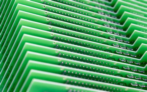
Challenges In Manufacturing High Frequency PCB Boards
The manufacturing of high-frequency printed circuit boards (PCBs) presents a unique set of challenges that distinguish it from the production of standard PCBs. As the demand for high-speed communication and advanced electronic devices continues to grow, the need for high-frequency PCBs has become increasingly critical. These boards are essential in applications such as telecommunications, aerospace, and advanced computing, where they facilitate the transmission of signals at microwave frequencies. However, the complexity of their design and production introduces several hurdles that manufacturers must overcome to ensure optimal performance and reliability.
One of the primary challenges in manufacturing high-frequency PCBs is the selection of suitable materials.
Unlike standard PCBs, which often use FR-4 as a substrate, high-frequency boards require materials with low dielectric constants and low loss tangents to minimize signal loss and distortion. Materials such as PTFE (polytetrafluoroethylene) and ceramic-filled laminates are commonly used, but they come with their own set of difficulties. These materials can be more expensive and harder to process, requiring specialized equipment and techniques to handle them effectively. Moreover, the thermal management of these materials is crucial, as they must maintain stability under varying temperature conditions to prevent performance degradation.
In addition to material selection, the precision of the manufacturing process is paramount.
High-frequency PCBs demand tighter tolerances and more precise etching to ensure that the signal paths are accurately defined. Any deviation in the dimensions of the traces can lead to impedance mismatches, which can severely affect the board’s performance. This necessitates the use of advanced fabrication technologies, such as laser direct imaging and controlled depth drilling, to achieve the required precision. Furthermore, the multilayer nature of many high-frequency PCBs adds another layer of complexity, as it requires meticulous alignment and lamination processes to ensure that all layers are correctly registered.
Another significant challenge is the integration of components on high-frequency PCBs.
The miniaturization of electronic components and the need for high-density interconnections can complicate the assembly process. Surface mount technology (SMT) is often employed, but it requires careful consideration of component placement and soldering techniques to avoid issues such as signal interference and thermal stress. Additionally, the testing and quality assurance of high-frequency PCBs are more demanding than those for standard boards. Specialized testing equipment is necessary to evaluate the performance of these boards at high frequencies, and any defects or inconsistencies must be identified and rectified to prevent failures in the field.
Moreover, the rapid pace of technological advancement poses an ongoing challenge for manufacturers.
As the frequency requirements of electronic devices continue to increase, PCB manufacturers must constantly innovate and adapt their processes to meet these evolving demands. This requires a commitment to research and development, as well as investment in new technologies and training for personnel.
In conclusion, the manufacturing of high-frequency PCBs is a complex and demanding process that requires careful consideration of materials, precision in fabrication, and meticulous assembly and testing. Despite these challenges, the continued advancement of technology and the growing demand for high-speed communication ensure that high-frequency PCBs will remain a critical component in the electronics industry. By addressing these challenges through innovation and expertise, manufacturers can continue to produce high-quality boards that meet the needs of modern applications.
Signal Integrity Considerations In High Frequency PCB Design
In the realm of high-frequency PCB design, signal integrity emerges as a critical consideration that can significantly impact the performance and reliability of electronic systems. As the demand for faster and more efficient electronic devices continues to grow, engineers are increasingly tasked with designing PCBs that can handle high-frequency signals without compromising signal integrity. This challenge necessitates a comprehensive understanding of the factors that influence signal integrity and the implementation of strategies to mitigate potential issues.
One of the primary concerns in high-frequency PCB design is the phenomenon of signal reflection, which occurs when a signal encounters an impedance discontinuity along its transmission path.
This can lead to signal degradation and data errors, particularly in high-speed applications. To address this, designers must ensure that the characteristic impedance of the transmission lines is matched to the source and load impedances. This involves careful selection of materials, such as low-loss dielectrics, and precise control over trace dimensions and spacing.
In addition to impedance matching, minimizing crosstalk is essential for maintaining signal integrity in high-frequency PCBs.
Crosstalk occurs when a signal in one trace induces an unwanted signal in an adjacent trace, potentially leading to data corruption. To mitigate crosstalk, designers can employ techniques such as increasing the spacing between traces, using differential signaling, and incorporating ground planes to provide a return path for signals. These strategies help to isolate signals and reduce electromagnetic interference, thereby preserving signal integrity.
Another critical aspect of high-frequency PCB design is the management of signal attenuation.
As frequency increases, signal attenuation becomes more pronounced due to factors such as dielectric losses and conductor losses. To combat this, designers can use materials with low dielectric constants and loss tangents, as well as optimize trace geometries to minimize resistance. Additionally, the use of via stubs should be minimized, as they can introduce unwanted inductance and capacitance, further contributing to signal attenuation.
Moreover, the role of power integrity cannot be overlooked in high-frequency PCB design.
Power integrity refers to the ability of the power distribution network to deliver stable and noise-free power to all components on the PCB. Inadequate power integrity can lead to voltage fluctuations and increased electromagnetic interference, which can adversely affect signal integrity. To ensure robust power integrity, designers should implement decoupling capacitors strategically, design power and ground planes with low inductance paths, and consider the use of power integrity simulation tools to identify potential issues early in the design process.
Thermal management is another consideration that intersects with signal integrity in high-frequency PCB design.
High-frequency operation often results in increased power dissipation, which can lead to elevated temperatures and affect the electrical properties of materials. Effective thermal management strategies, such as the use of thermal vias, heat sinks, and proper airflow design, are essential to maintain optimal operating conditions and prevent thermal-induced signal degradation.
In conclusion, maintaining signal integrity in high-frequency PCB design requires a multifaceted approach that addresses impedance matching, crosstalk reduction, signal attenuation, power integrity, and thermal management. By understanding and implementing these considerations, designers can create high-frequency PCBs that deliver reliable performance and meet the demands of modern electronic applications. As technology continues to advance, the importance of signal integrity in high-frequency PCB design will only grow, underscoring the need for ongoing research and innovation in this field.


