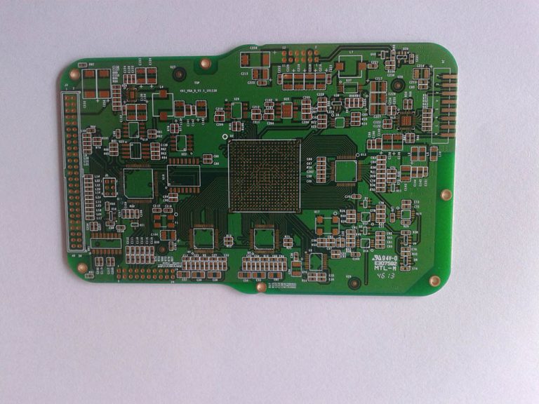
High frequency pcb design guidelines
Understanding Material Selection for High Frequency PCB Design
In the realm of high frequency printed circuit board (PCB) design, the selection of materials plays a pivotal role in determining the performance and reliability of the final product. As electronic devices continue to evolve, operating at increasingly higher frequencies, the demand for precise and efficient PCB designs has never been more critical. Understanding the nuances of material selection is essential for engineers and designers aiming to optimize their high frequency applications.
To begin with, the dielectric constant (Dk) of the substrate material is a fundamental parameter that influences signal integrity in high frequency PCBs.
A lower dielectric constant is generally preferred as it allows for faster signal propagation and reduced signal loss. Materials such as PTFE (polytetrafluoroethylene) and certain ceramic-filled laminates are often chosen for their low Dk values, which are conducive to high-speed signal transmission. However, it is crucial to balance the dielectric constant with other material properties to ensure overall performance.
In addition to the dielectric constant, the dissipation factor (Df) is another critical consideration.
The dissipation factor measures the inherent energy loss within the material as signals pass through it. A lower dissipation factor indicates that the material is more efficient at transmitting high frequency signals with minimal loss. This is particularly important in applications where signal integrity is paramount, such as in telecommunications and radar systems. Materials with low Df values, like certain advanced laminates, are often selected to minimize energy loss and maintain signal clarity.
Thermal management is another aspect that cannot be overlooked in high frequency PCB design.
As frequencies increase, so does the potential for heat generation, which can adversely affect the performance and longevity of the PCB. Therefore, materials with good thermal conductivity are essential to dissipate heat effectively. Copper-clad laminates with enhanced thermal properties are frequently used to address this challenge, ensuring that the PCB can operate efficiently under high thermal loads.
Moreover, the coefficient of thermal expansion (CTE) is a vital factor in material selection.
A mismatch in CTE between the substrate and other components can lead to mechanical stress and potential failure during thermal cycling. Selecting materials with a CTE that closely matches that of the components can mitigate these risks, enhancing the reliability of the PCB in high frequency applications.
Furthermore, the choice of materials must also consider manufacturability and cost-effectiveness.
While high-performance materials offer superior electrical and thermal properties, they can be more challenging to process and may incur higher costs. It is essential to strike a balance between performance requirements and practical considerations, ensuring that the chosen materials can be efficiently integrated into the manufacturing process without exceeding budget constraints.
In conclusion, the selection of materials for high frequency PCB design is a complex but crucial task that requires careful consideration of various electrical, thermal, and mechanical properties. By understanding the interplay between these factors, designers can make informed decisions that enhance the performance and reliability of their high frequency applications. As technology continues to advance, the importance of meticulous material selection in high frequency PCB design will only grow, underscoring its significance in the development of cutting-edge electronic devices.
Best Practices for Signal Integrity in High Frequency PCBs
In the realm of high frequency printed circuit board (PCB) design, ensuring signal integrity is paramount. As electronic devices become more sophisticated and operate at higher frequencies, the challenges associated with maintaining signal integrity grow increasingly complex. To address these challenges, designers must adhere to a set of best practices that mitigate potential issues and enhance the performance of high frequency PCBs.
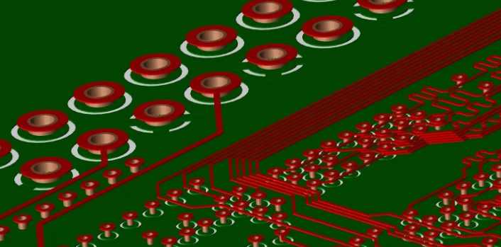
One of the fundamental considerations in high frequency PCB design is the management of impedance.
Impedance mismatches can lead to signal reflections, which degrade signal quality and can cause data errors. To prevent this, it is crucial to maintain consistent impedance throughout the signal path. This can be achieved by carefully designing the trace widths and spacing, as well as selecting appropriate materials with consistent dielectric properties. Additionally, employing controlled impedance techniques, such as using microstrip or stripline configurations, can further enhance signal integrity.
Transitioning to another critical aspect, the layout of the PCB plays a significant role in signal integrity.
High frequency signals are particularly susceptible to electromagnetic interference (EMI) and crosstalk, which can be exacerbated by poor layout practices. To minimize these effects, designers should prioritize the use of ground planes, which provide a return path for signals and help shield them from external interference. Moreover, keeping signal traces as short as possible and routing them away from noisy components can significantly reduce the risk of crosstalk and EMI.
In addition to layout considerations, the choice of materials is another vital factor in high frequency PCB design.
The dielectric constant and loss tangent of the substrate material can greatly influence signal propagation. Materials with low dielectric constants and loss tangents are preferred, as they reduce signal attenuation and dispersion. Furthermore, selecting materials with stable properties over a wide frequency range ensures consistent performance across different operating conditions.
As we delve deeper into the intricacies of high frequency PCB design, it becomes evident that power integrity is closely linked to signal integrity.
Inadequate power distribution can lead to voltage fluctuations, which in turn affect signal quality. To address this, designers should implement robust power distribution networks (PDNs) that minimize voltage drops and provide stable power to all components. Utilizing decoupling capacitors strategically placed near power pins can also help filter out noise and maintain a clean power supply.
Moreover, the integration of simulation tools into the design process is an invaluable practice for ensuring signal integrity.
These tools allow designers to model and analyze the behavior of high frequency signals within the PCB, identifying potential issues before physical prototypes are built. By simulating various scenarios, designers can optimize trace routing, impedance matching, and other critical parameters, ultimately leading to a more reliable and efficient design.
In conclusion, maintaining signal integrity in high frequency PCB design requires a comprehensive approach that encompasses impedance management, thoughtful layout practices, careful material selection, and robust power distribution. By adhering to these best practices, designers can mitigate the challenges associated with high frequency operation and ensure the reliable performance of their electronic devices. As technology continues to advance, the importance of these guidelines will only grow, underscoring the need for meticulous attention to detail in every aspect of high frequency PCB design.
Thermal Management Techniques in High Frequency PCB Design
In the realm of high frequency PCB design, thermal management emerges as a critical consideration, given the intricate interplay between electrical performance and heat dissipation. As electronic devices continue to shrink in size while increasing in functionality, the demand for efficient thermal management techniques becomes paramount. High frequency circuits, characterized by rapid signal transitions and high power densities, generate significant amounts of heat. If not properly managed, this heat can lead to performance degradation, component failure, and reduced reliability of the entire system. Therefore, understanding and implementing effective thermal management strategies is essential for ensuring the longevity and efficiency of high frequency PCBs.
One of the primary techniques in thermal management is the use of thermal vias
These are strategically placed to facilitate the transfer of heat from the surface of the PCB to the inner layers or to an external heat sink. By providing a direct path for heat to dissipate, thermal vias help in maintaining the temperature of critical components within safe operating limits. Moreover, the integration of thermal vias must be carefully planned to avoid interference with the electrical performance of the PCB, ensuring that they do not disrupt signal integrity or increase electromagnetic interference.
In addition to thermal vias, the selection of appropriate materials plays a crucial role in thermal management.
High frequency PCBs often utilize materials with high thermal conductivity, such as copper, to enhance heat dissipation. The choice of substrate material is equally important, as it affects both the thermal and electrical properties of the PCB. Materials like FR-4, while commonly used, may not always provide the best thermal performance for high frequency applications. Instead, advanced materials such as Rogers or ceramic-based substrates may be employed to achieve better thermal management without compromising on electrical performance.
Furthermore, the design of the PCB layout itself can significantly impact thermal management.
Components that generate substantial heat should be placed in areas where heat can be effectively dissipated, such as near the edges of the board or in proximity to heat sinks. Additionally, the use of thermal pads and heat spreaders can aid in distributing heat more evenly across the PCB, preventing localized hotspots that could lead to component failure. The layout should also consider airflow, ensuring that there is adequate ventilation to carry away excess heat.
Another technique involves the use of active cooling methods, such as fans or liquid cooling systems, particularly in high-power applications where passive cooling may not suffice. While these methods can be highly effective, they also introduce additional complexity and cost to the design. Therefore, a careful cost-benefit analysis is necessary to determine the most appropriate cooling solution for a given application.
In conclusion, thermal management in high frequency PCB design is a multifaceted challenge that requires a comprehensive approach.
By employing a combination of thermal vias, selecting suitable materials, optimizing PCB layout, and considering active cooling solutions, designers can effectively manage heat dissipation. This not only enhances the performance and reliability of high frequency PCBs but also extends their operational lifespan. As technology continues to evolve, the importance of robust thermal management techniques will only grow, underscoring the need for ongoing innovation and adaptation in PCB design practices.

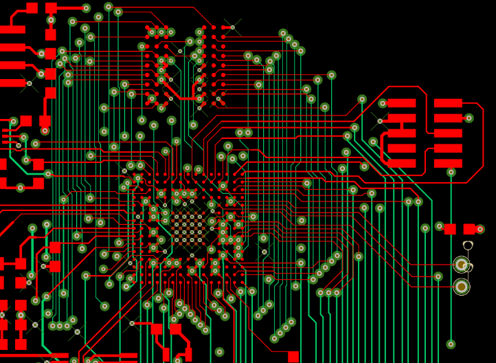
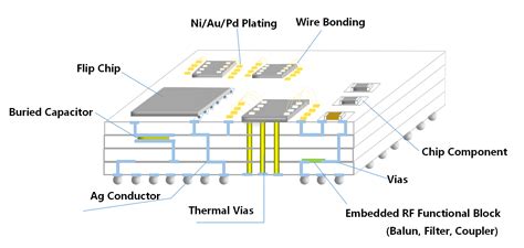
Layer Stackup Considerations for High Frequency PCB Applications
In the realm of high frequency PCB design, the layer stackup plays a pivotal role in determining the performance and reliability of the final product. As electronic devices continue to evolve, operating at increasingly higher frequencies, the need for meticulous attention to layer stackup considerations becomes paramount. The stackup not only influences the electrical performance but also impacts the manufacturability and cost-effectiveness of the PCB. Therefore, understanding the intricacies of layer stackup is essential for engineers and designers working in high frequency applications.
To begin with, the choice of materials is a critical factor in high frequency PCB design.
The dielectric material used between the layers significantly affects signal integrity, as it determines the dielectric constant and loss tangent, both of which are crucial for high frequency performance. Materials with low dielectric constants and low loss tangents are preferred, as they minimize signal loss and dispersion. Furthermore, the thickness of the dielectric layers must be carefully selected to ensure controlled impedance, which is vital for maintaining signal integrity at high frequencies.
Transitioning to the arrangement of layers, it is important to consider the distribution of signal, power, and ground layers within the stackup.
A well-designed stackup typically alternates signal layers with ground or power planes, which helps in reducing electromagnetic interference (EMI) and crosstalk. This configuration also aids in providing a clear return path for signals, thereby enhancing signal integrity. Additionally, the proximity of signal layers to ground planes can significantly affect the impedance and should be optimized to match the characteristic impedance of the transmission lines.
Moreover, the number of layers in the stackup is another crucial consideration.
While adding more layers can provide greater flexibility in routing and improve signal integrity, it also increases the complexity and cost of the PCB. Therefore, a balance must be struck between performance requirements and budget constraints. In high frequency applications, it is often beneficial to use a multi-layer stackup to separate high-speed signals from low-speed ones, thereby minimizing interference and ensuring optimal performance.
Another aspect to consider is the thermal management of the PCB.
High frequency applications often generate significant amounts of heat, which can adversely affect the performance and reliability of the board. Therefore, the stackup should be designed to facilitate efficient heat dissipation. This can be achieved by incorporating thermal vias and using materials with good thermal conductivity. Additionally, the placement of power and ground planes can aid in spreading heat evenly across the board, thereby preventing hotspots.
In conclusion, the layer stackup is a fundamental aspect of high frequency PCB design that requires careful consideration and planning. By selecting appropriate materials, optimizing layer arrangement, balancing the number of layers, and addressing thermal management, designers can ensure that their high frequency PCBs meet the desired performance and reliability standards. As technology continues to advance, the importance of a well-designed layer stackup will only grow, making it an indispensable element in the toolkit of any PCB designer working in high frequency applications. Through meticulous attention to these guidelines, engineers can successfully navigate the complexities of high frequency PCB design and deliver cutting-edge solutions that meet the demands of modern electronic devices.