High-Frequency PCB Interference Issues and Solutions
Introduction
As electronic devices continue to operate at increasingly higher frequencies, printed circuit board (PCB) designers face growing challenges with interference issues. High-frequency PCBs, typically those operating above 50 MHz, are particularly susceptible to various forms of electromagnetic interference (EMI) that can degrade signal integrity, reduce system reliability, and cause compliance failures with electromagnetic compatibility (EMC) regulations. This article examines the primary interference problems encountered in high-frequency PCB design and provides practical solutions to mitigate these issues.
1. Understanding High-Frequency PCB Interference
1.1 Types of Interference in High-Frequency PCBs
High-frequency PCBs experience several distinct interference phenomena:
- Crosstalk: Unwanted coupling between adjacent traces or components
- Ground Bounce: Voltage fluctuations in ground reference planes
- Power Plane Noise: Disturbances in power distribution networks
- Radiated Emissions: Unintentional electromagnetic radiation from the board
- Signal Integrity Issues: Reflections, ringing, and timing errors
- Skin Effect: Current concentration at conductor surfaces at high frequencies
1.2 Frequency Considerations
The behavior of interference changes significantly with frequency:
- Below 1 MHz: Primarily conducted emissions concerns
- 1 MHz to 30 MHz: Transition region with both conducted and radiated emissions
- Above 30 MHz: Dominantly radiated emissions problems
- Above 1 GHz: Wavelength approaches physical board dimensions, creating wave propagation effects
2. Major Interference Mechanisms
2.1 Transmission Line Effects
At high frequencies, PCB traces behave as transmission lines rather than simple conductors. When the trace length approaches 1/10 of the signal wavelength, impedance matching becomes critical to prevent:
- Signal reflections due to impedance mismatches
- Standing waves that create uneven voltage distributions
- Timing skew between related signals
2.2 Parasitic Elements
Unintentional parasitic components become significant at high frequencies:
- Parasitic capacitance (typically 0.1-1 pF/cm between adjacent traces)
- Parasitic inductance (approximately 1 nH/mm for typical traces)
- Via inductance (0.2-0.5 nH per via)
2.3 Return Path Discontinuities
High-frequency currents follow the path of least inductance (not necessarily least resistance), making return path continuity essential. Common problems include:
- Split planes beneath high-speed signals
- Insufficient ground vias in multilayer boards
- Long return paths creating ground loops
3. Key Solutions for High-Frequency Interference
3.1 Proper Stackup Design
A well-designed layer stackup is fundamental for high-frequency performance:
- Use symmetrical stackups to prevent warping and maintain impedance control
- Provide adjacent power and ground planes for decoupling
- Implement microstrip or stripline routing for controlled impedance signals
- Maintain thin dielectrics (typically 2-4 mil) for high-speed signals
Recommended 8-layer stackup example:
- Signal (microstrip)
- Ground plane
- Signal (stripline)
- Power plane
- Power plane
- Signal (stripline)
- Ground plane
- Signal (microstrip)
3.2 Impedance Control Techniques
- Calculate trace dimensions for target impedance (50Ω or 75Ω typical)
- Use field solvers for accurate impedance modeling
- Maintain consistent dielectric thickness around controlled impedance traces
- Avoid abrupt width changes that create impedance discontinuities
3.3 Effective Grounding Strategies
- Use solid ground planes (avoid split planes under high-speed signals)
- Implement via stitching (1 via every λ/10 at highest frequency)
- Separate analog and digital grounds with proper bridging
- Minimize ground loop areas by providing direct return paths
3.4 Power Integrity Management
- Use multiple decoupling capacitors (mix of bulk, ceramic, and high-frequency)
- Implement power plane pairs with thin dielectrics
- Apply proper capacitor placement (smallest value closest to IC)
- Use power island techniques for sensitive circuits
3.5 Signal Routing Best Practices
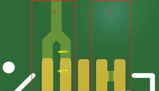
- Follow the 3W rule (trace spacing ≥ 3× trace width) to reduce crosstalk
- Route differential pairs properly (maintain consistent spacing and length matching)
- Avoid right-angle bends (use 45° or curved traces)
- Implement length matching for critical parallel buses
- Use via optimization (back-drilling, microvias for HDI designs)
3.6 Shielding and Containment
- Implement board-level shielding (copper pours, shielding cans)
- Use guard traces around sensitive signals
- Apply conductive coatings for enclosure shielding
- Properly terminate cables at board interfaces
4. Advanced Techniques for Extreme High Frequency
For designs operating above 1 GHz, additional measures become necessary:
4.1 Material Selection
- Low-Dk materials (Rogers, Isola high-frequency laminates)
- Low-loss dielectrics (tan δ < 0.005 at operating frequency)
- Smooth copper foils to reduce skin effect losses
4.2 3D Electromagnetic Simulation
- Full-wave solvers for accurate modeling
- S-parameter extraction for interconnects
- Power integrity analysis with frequency-domain tools
4.3 Advanced Packaging Techniques
- Embedded components to reduce parasitics
- Chip-on-board (COB) for shortest interconnects
- Silicon interposers for ultra-high density
5. Testing and Validation
5.1 Measurement Techniques
- Time Domain Reflectometry (TDR) for impedance verification
- Vector Network Analysis (VNA) for S-parameter measurement
- Near-field scanning for EMI hotspot identification
5.2 Compliance Testing
- Radiated emissions testing (FCC, CISPR standards)
- Conducted emissions testing
- Immunity testing (ESD, EFT, surge)
Conclusion
High-frequency PCB interference presents complex challenges that require careful consideration throughout the design process. By understanding the fundamental interference mechanisms and implementing proper design techniques—including controlled impedance routing, optimized stackups, careful grounding, and power integrity management—designers can successfully mitigate interference issues in high-frequency designs. As operating frequencies continue to increase with 5G, IoT, and high-performance computing applications, these techniques will become increasingly critical for successful product development.
The most effective approach combines proper design methodology with thorough simulation and testing. Investing in these areas during the design phase prevents costly redesigns and ensures reliable operation of high-frequency electronic systems. Future developments in materials, simulation tools, and manufacturing techniques will continue to push the boundaries of high-frequency PCB performance while maintaining acceptable interference levels.