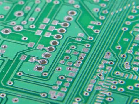
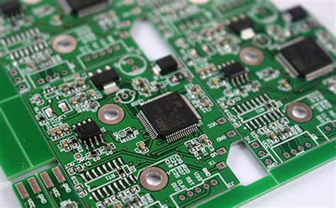
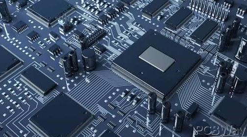
High frequency pcb layout
Understanding Signal Integrity in High Frequency PCB Layout
In the realm of high-frequency printed circuit board (PCB) design, understanding signal integrity is paramount to ensuring optimal performance and reliability. As electronic devices become increasingly complex and operate at higher frequencies, the challenges associated with maintaining signal integrity grow correspondingly. Signal integrity refers to the quality and reliability of electrical signals as they travel through a PCB. In high-frequency applications, even minor disruptions can lead to significant performance degradation, making it crucial for designers to meticulously consider various factors during the layout process.
One of the primary considerations in high-frequency PCB layout is impedance control.
Impedance, the resistance to the flow of alternating current, must be carefully managed to prevent signal reflections and losses. To achieve this, designers often employ controlled impedance traces, which involve precise calculations of trace width, spacing, and the dielectric properties of the substrate material. By ensuring that the impedance is consistent throughout the signal path, designers can minimize reflections and maintain signal integrity.
Moreover, the layout of high-frequency PCBs must account for the effects of parasitic capacitance and inductance.
These unwanted elements can introduce signal distortion and crosstalk, which is the undesired coupling of signals between adjacent traces. To mitigate these effects, designers often use techniques such as increasing the spacing between traces, employing ground planes, and utilizing differential signaling. Differential signaling, in particular, is effective in reducing electromagnetic interference (EMI) and enhancing signal integrity by transmitting signals over two complementary traces.
Transitioning to another critical aspect, the choice of materials plays a significant role in high-frequency PCB design.
The dielectric constant and loss tangent of the substrate material can significantly impact signal propagation. Materials with low dielectric constants and loss tangents are preferred for high-frequency applications as they reduce signal attenuation and dispersion. Additionally, the use of low-loss materials can help maintain signal integrity over longer distances, which is particularly important in applications such as telecommunications and high-speed data transmission.
Thermal management is another crucial factor in maintaining signal integrity in high-frequency PCBs.
As frequencies increase, so does the potential for heat generation, which can adversely affect the performance of the board. Effective thermal management strategies, such as the use of thermal vias, heat sinks, and proper component placement, are essential to dissipate heat and prevent thermal-induced signal degradation.
Furthermore, the integration of simulation tools into the design process can greatly enhance the understanding and management of signal integrity issues.
These tools allow designers to model and analyze the behavior of signals within the PCB, providing insights into potential problem areas and enabling the optimization of the layout before physical prototyping. By leveraging simulation, designers can identify and address issues such as signal reflections, crosstalk, and impedance mismatches early in the design process, thereby reducing the risk of costly revisions.
In conclusion, maintaining signal integrity in high-frequency PCB layout requires a comprehensive understanding of various factors, including impedance control, parasitic effects, material selection, thermal management, and the use of simulation tools. By carefully considering these elements, designers can ensure that their high-frequency PCBs perform reliably and efficiently, meeting the demands of modern electronic applications. As technology continues to advance, the importance of signal integrity in high-frequency PCB design will only grow, underscoring the need for ongoing research and innovation in this critical field.
Best Practices for Designing High Frequency PCB Layouts
Designing high-frequency printed circuit board (PCB) layouts requires a meticulous approach to ensure optimal performance and reliability. As electronic devices continue to evolve, the demand for high-frequency applications has increased, necessitating a deeper understanding of the intricacies involved in PCB design. To achieve the desired outcomes, it is essential to adhere to best practices that address the unique challenges posed by high-frequency signals.
One of the fundamental considerations in high-frequency PCB design is the management of signal integrity.
High-frequency signals are particularly susceptible to issues such as signal reflection, crosstalk, and electromagnetic interference (EMI). To mitigate these problems, it is crucial to maintain controlled impedance throughout the PCB. This can be achieved by carefully selecting the dielectric material and maintaining consistent trace widths and spacing. Additionally, employing differential signaling can help reduce the impact of noise and improve signal integrity.
Transitioning to another critical aspect, the layout of the ground plane plays a pivotal role in high-frequency PCB design.
A solid and continuous ground plane is essential for providing a low-impedance return path for high-frequency signals. This not only minimizes EMI but also enhances the overall performance of the circuit. It is advisable to avoid splitting the ground plane, as this can lead to increased inductance and potential signal integrity issues. Furthermore, ensuring that the ground plane is as close as possible to the signal traces can help reduce loop inductance and improve signal quality.
In addition to ground plane considerations, the placement of components is another vital factor in high-frequency PCB design.
Components should be strategically placed to minimize the length of high-frequency signal paths. This reduces the potential for signal degradation and EMI. Grouping related components together and placing them in close proximity can also help achieve this goal. Moreover, it is important to consider the orientation of components to minimize parasitic capacitance and inductance, which can adversely affect high-frequency performance.
As we delve deeper into the intricacies of high-frequency PCB design, the importance of proper power distribution cannot be overstated.
Ensuring a stable power supply is crucial for maintaining signal integrity and minimizing noise. To achieve this, designers should implement a robust power distribution network (PDN) with adequate decoupling capacitors placed close to the power pins of integrated circuits. This helps to filter out high-frequency noise and provides a stable voltage supply to the components.
Furthermore, the use of vias in high-frequency PCB layouts requires careful consideration.
While vias are necessary for connecting different layers of a PCB, they can introduce unwanted inductance and capacitance, which can degrade signal quality. To minimize these effects, it is advisable to use as few vias as possible in high-frequency signal paths. When vias are unavoidable, using blind or buried vias can help reduce their impact on signal integrity.
In conclusion, designing high-frequency PCB layouts demands a comprehensive understanding of the factors that influence signal integrity and performance. By adhering to best practices such as maintaining controlled impedance, optimizing ground plane layout, strategic component placement, ensuring proper power distribution, and minimizing the use of vias, designers can create high-frequency PCBs that meet the stringent requirements of modern electronic applications. As technology continues to advance, staying informed about the latest design techniques and materials will be essential for achieving success in high-frequency PCB design.

Challenges and Solutions in High Frequency PCB Layout Design
Designing high frequency printed circuit boards (PCBs) presents a unique set of challenges that require careful consideration and meticulous planning. As electronic devices continue to evolve, the demand for high frequency applications has surged, necessitating PCB layouts that can accommodate these advanced requirements. The primary challenge in high frequency PCB design lies in managing signal integrity, which is crucial for ensuring that the signals transmitted across the board maintain their integrity without distortion or loss. This is particularly important as frequencies increase, since higher frequencies are more susceptible to issues such as electromagnetic interference (EMI) and crosstalk.
To address these challenges, designers must employ a variety of strategies.
One fundamental approach is to minimize the length of signal paths. Shorter paths reduce the potential for signal degradation and help maintain signal integrity. Additionally, the use of controlled impedance traces is essential. By carefully designing the width and spacing of traces, designers can ensure that the impedance remains consistent, which is critical for high frequency signals. This involves selecting the appropriate materials and layer stack-ups to achieve the desired impedance levels.
Another significant challenge in high frequency PCB layout is managing EMI.
High frequency signals can easily radiate electromagnetic energy, which can interfere with other components on the board or even with external devices. To mitigate this, designers often incorporate ground planes and shielding techniques. Ground planes provide a return path for signals and help reduce EMI by acting as a barrier. Shielding, on the other hand, involves enclosing sensitive components or traces with conductive materials to prevent interference.
Crosstalk, the unwanted coupling of signals between adjacent traces, is another issue that becomes more pronounced at high frequencies.
To combat crosstalk, designers can increase the spacing between traces or use differential signaling. Differential signaling involves using pairs of traces to carry signals, which helps cancel out noise and reduces the impact of crosstalk. Additionally, careful layer management in the PCB stack-up can help isolate high frequency signals from other parts of the circuit, further minimizing crosstalk.
Thermal management is also a critical consideration in high frequency PCB design.
As frequencies increase, so does the power consumption, leading to higher heat generation. Effective thermal management strategies, such as the use of thermal vias, heat sinks, and proper component placement, are essential to ensure that the board operates within safe temperature limits. This not only enhances performance but also prolongs the lifespan of the components.
In conclusion, high frequency PCB layout design is a complex process that requires a deep understanding of various factors that can affect signal integrity and overall performance. By employing strategies such as minimizing signal path lengths, using controlled impedance traces, managing EMI and crosstalk, and implementing effective thermal management, designers can overcome the challenges associated with high frequency applications. As technology continues to advance, the demand for high frequency PCBs will only grow, making it imperative for designers to stay abreast of the latest techniques and tools available to tackle these challenges effectively. Through careful planning and execution, it is possible to create high frequency PCB layouts that meet the stringent requirements of modern electronic devices, ensuring reliable and efficient operation.

Material Selection for High Frequency PCB Layouts
In the realm of high frequency printed circuit board (PCB) design, the selection of materials plays a pivotal role in determining the overall performance and reliability of the final product. As electronic devices continue to evolve, operating at increasingly higher frequencies, the demand for precise and efficient PCB layouts has never been more critical. Consequently, understanding the nuances of material selection becomes essential for engineers and designers striving to optimize their high frequency applications.
To begin with, one must consider the dielectric constant (Dk) of the substrate material, as it significantly influences signal integrity and impedance control.
Materials with a low and stable dielectric constant are preferred for high frequency applications because they minimize signal loss and ensure consistent signal propagation. For instance, polytetrafluoroethylene (PTFE) and ceramic-filled laminates are popular choices due to their low Dk values and excellent high frequency performance. These materials help maintain signal integrity by reducing the potential for signal distortion and attenuation, which are common challenges in high frequency circuits.
In addition to the dielectric constant, the dissipation factor (Df) of the material is another critical parameter to consider.
The dissipation factor measures the inherent energy loss within the substrate material as signals pass through it. A low dissipation factor is desirable for high frequency PCBs, as it indicates minimal energy loss, thereby enhancing the efficiency of the circuit. Materials such as Rogers RO4000 series and Taconic RF-35 are often selected for their low dissipation factors, which contribute to reduced signal loss and improved overall performance.
Moreover, thermal management is a crucial aspect of high frequency PCB design, as excessive heat can lead to performance degradation and potential failure of the circuit.
Therefore, selecting materials with good thermal conductivity is vital to ensure efficient heat dissipation. High frequency applications often employ materials like aluminum-backed laminates or those with embedded heat spreaders to effectively manage thermal loads. These materials help maintain the operational stability of the circuit by preventing overheating and ensuring consistent performance over time.
Furthermore, the coefficient of thermal expansion (CTE) is an important consideration, particularly in applications where temperature fluctuations are common.
A material with a low CTE ensures dimensional stability, reducing the risk of mechanical stress and potential damage to the PCB. This is especially important in high frequency applications where precise alignment of components is critical. Materials such as ceramic-filled PTFE offer low CTE values, making them suitable for environments with varying temperatures.
Additionally, the choice of copper cladding is another factor that influences the performance of high frequency PCBs.
The thickness and quality of the copper layer can affect signal transmission and power handling capabilities. Thinner copper layers are often preferred for high frequency applications to minimize skin effect losses, which occur when high frequency signals travel primarily on the surface of the conductor. However, the copper must also be of high purity and uniformity to ensure consistent electrical performance.
In conclusion, the selection of materials for high frequency PCB layouts is a multifaceted process that requires careful consideration of various parameters, including dielectric constant, dissipation factor, thermal management, coefficient of thermal expansion, and copper cladding. By meticulously evaluating these factors, engineers and designers can optimize their PCB designs to meet the demanding requirements of high frequency applications, ultimately ensuring superior performance and reliability in the final product.