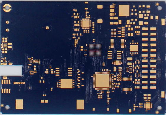
High frequency pcb traces
Understanding Signal Integrity in High Frequency PCB Traces
In the realm of modern electronics, the demand for high-speed communication and processing has led to the proliferation of high frequency printed circuit boards (PCBs). These PCBs are integral to the performance of a wide array of devices, from smartphones to advanced computing systems. A critical aspect of designing these high frequency PCBs is ensuring signal integrity, which is paramount for the reliable operation of electronic circuits. Signal integrity refers to the preservation of the quality of electrical signals as they traverse through the PCB traces. As frequencies increase, maintaining signal integrity becomes increasingly challenging due to various factors that can distort or degrade the signal.
One of the primary concerns in high frequency PCB design is the impedance of the traces.
Impedance is the measure of opposition that a circuit presents to the flow of alternating current and is influenced by the trace width, thickness, and the dielectric material of the PCB. To ensure signal integrity, it is crucial to maintain a consistent impedance along the trace. Variations in impedance can lead to reflections, which can cause signal distortion and data errors. Therefore, careful consideration of trace geometry and material properties is essential in the design phase.
Moreover, as frequencies rise, the skin effect becomes more pronounced.
The skin effect is a phenomenon where alternating current tends to flow near the surface of a conductor rather than through its entire cross-section. This effect increases the effective resistance of the trace at higher frequencies, which can lead to signal attenuation. To mitigate this, designers often use wider traces or employ materials with lower resistivity to reduce the impact of the skin effect.
In addition to impedance and the skin effect, crosstalk is another significant issue that can affect signal integrity in high frequency PCBs.
Crosstalk occurs when a signal in one trace induces an unwanted signal in an adjacent trace, leading to interference. This is particularly problematic in densely packed PCBs where traces are in close proximity. To minimize crosstalk, designers can increase the spacing between traces, use ground planes to shield signals, or employ differential signaling techniques.
Furthermore, the dielectric properties of the PCB material play a crucial role in signal integrity.
The dielectric constant and loss tangent of the material affect the speed and attenuation of signals. Materials with a low dielectric constant and loss tangent are preferred for high frequency applications as they allow signals to propagate with minimal loss. Selecting the appropriate dielectric material is therefore a key consideration in the design of high frequency PCBs.
Additionally, via design is another factor that can impact signal integrity.
Vias are used to connect different layers of a PCB, but they can introduce inductance and capacitance that affect high frequency signals. To minimize these effects, designers can use techniques such as back-drilling to remove unused via stubs or employ blind and buried vias to reduce parasitic elements.
In conclusion, understanding and addressing the factors that affect signal integrity is essential for the successful design of high frequency PCB traces. By carefully considering impedance, the skin effect, crosstalk, dielectric properties, and via design, engineers can ensure that their PCBs perform reliably at high frequencies. As technology continues to advance, the importance of maintaining signal integrity in high frequency applications will only grow, making it a critical area of focus for PCB designers.
Design Techniques for Minimizing Crosstalk in High Frequency PCB Traces
In the realm of high-frequency printed circuit board (PCB) design, minimizing crosstalk is a critical consideration that can significantly impact the performance and reliability of electronic systems. Crosstalk, the unwanted coupling of signals between adjacent traces, can lead to signal integrity issues, increased electromagnetic interference, and degraded system performance. Therefore, understanding and implementing effective design techniques to mitigate crosstalk is essential for engineers working with high-frequency PCBs.
To begin with, one of the fundamental strategies for minimizing crosstalk is to carefully manage the physical layout of the PCB traces.
By increasing the spacing between adjacent traces, designers can reduce the capacitive and inductive coupling that contributes to crosstalk. This approach is particularly effective in high-frequency applications where the wavelength of the signals is comparable to the trace dimensions. Additionally, employing a ground plane between signal layers can further isolate traces and provide a return path for signals, thereby reducing the potential for crosstalk.
Moreover, the use of differential signaling is another effective technique for minimizing crosstalk in high-frequency PCBs.
Differential pairs, which consist of two traces carrying equal and opposite signals, are less susceptible to external noise and crosstalk. This is because any interference that affects one trace is likely to affect the other trace equally, allowing the differential receiver to cancel out the noise. Consequently, differential signaling is widely used in high-speed data communication applications where signal integrity is paramount.
In addition to layout considerations, the choice of materials and stack-up configuration plays a crucial role in crosstalk mitigation.
High-frequency PCBs often utilize low-loss dielectric materials that exhibit minimal signal attenuation and dispersion. These materials help maintain signal integrity over long trace lengths and reduce the potential for crosstalk. Furthermore, a well-designed stack-up with alternating signal and ground layers can enhance signal isolation and minimize electromagnetic interference.
Transitioning to another important aspect, the implementation of proper termination techniques is vital in controlling crosstalk.
Impedance mismatches at the ends of traces can lead to signal reflections, which exacerbate crosstalk. By employing appropriate termination resistors, designers can match the impedance of the traces to the source and load, thereby minimizing reflections and improving signal integrity. This technique is particularly important in high-frequency applications where signal reflections can significantly degrade performance.
Furthermore, the use of vias, which are vertical interconnections between different layers of a PCB, should be carefully managed to minimize crosstalk.
Vias can introduce parasitic inductance and capacitance, which can couple signals between layers and contribute to crosstalk. To mitigate this, designers should minimize the number of vias in high-frequency signal paths and ensure that return paths are properly managed to reduce loop areas.
In conclusion, minimizing crosstalk in high-frequency PCB traces requires a comprehensive approach that encompasses careful layout design, material selection, termination techniques, and via management. By implementing these strategies, engineers can enhance signal integrity, reduce electromagnetic interference, and ensure the reliable performance of high-frequency electronic systems. As technology continues to advance and the demand for high-speed communication grows, the importance of effective crosstalk mitigation techniques in PCB design will only become more pronounced.

Material Selection for Optimal Performance in High Frequency PCB Traces
In the realm of high-frequency printed circuit boards (PCBs), the selection of materials plays a pivotal role in determining the overall performance and reliability of the circuit. As electronic devices continue to evolve, operating at increasingly higher frequencies, the demand for materials that can support these frequencies without compromising signal integrity has become more pronounced. Consequently, understanding the properties and implications of various materials is essential for engineers and designers aiming to optimize high-frequency PCB traces.
To begin with, one of the most critical factors in material selection is the dielectric constant (Dk).
The dielectric constant affects the speed at which signals propagate through the PCB material. Materials with a lower dielectric constant are generally preferred for high-frequency applications because they allow signals to travel faster, thereby reducing signal delay. Moreover, a consistent dielectric constant across the material is crucial to ensure uniform signal propagation, minimizing the risk of signal distortion.
In addition to the dielectric constant, the dissipation factor (Df) is another key consideration.
The dissipation factor measures the dielectric losses in the material, which can lead to signal attenuation. For high-frequency applications, materials with a low dissipation factor are desirable as they minimize energy loss, thereby preserving signal strength over longer distances. This is particularly important in applications such as telecommunications and radar systems, where maintaining signal integrity is paramount.
Furthermore, the thermal properties of the material cannot be overlooked.
High-frequency circuits often generate significant amounts of heat, and materials with poor thermal management can lead to overheating and potential failure of the PCB. Therefore, selecting materials with good thermal conductivity and stability is essential to ensure the longevity and reliability of the circuit. Materials such as PTFE (polytetrafluoroethylene) and ceramics are often favored for their excellent thermal properties, making them suitable candidates for high-frequency applications.
Another aspect to consider is the material’s mechanical properties, including its ability to withstand environmental stresses such as vibration and mechanical shock.
High-frequency PCBs are frequently used in demanding environments, and materials that offer robust mechanical strength can prevent physical damage and maintain circuit integrity. Additionally, the material’s compatibility with manufacturing processes, such as lamination and etching, should be evaluated to ensure efficient production without compromising quality.
Transitioning to the topic of cost, it is important to balance performance requirements with budget constraints.
While high-performance materials like PTFE and ceramics offer superior electrical and thermal properties, they can be significantly more expensive than traditional FR-4 materials. Therefore, a cost-benefit analysis is essential to determine the most suitable material that meets both performance and budgetary needs.
In conclusion, the selection of materials for high-frequency PCB traces is a complex process that requires careful consideration of various electrical, thermal, mechanical, and economic factors. By understanding the implications of each material property, engineers and designers can make informed decisions that enhance the performance and reliability of high-frequency circuits. As technology continues to advance, the development of new materials and innovations in material science will undoubtedly play a crucial role in meeting the ever-growing demands of high-frequency applications.

The Role of Impedance Matching in High Frequency PCB Trace Design
In the realm of high-frequency printed circuit board (PCB) design, the concept of impedance matching plays a pivotal role in ensuring signal integrity and optimal performance. As electronic devices continue to evolve, operating at increasingly higher frequencies, the challenges associated with maintaining signal quality become more pronounced. Impedance matching, therefore, emerges as a critical consideration in the design of high-frequency PCB traces, as it directly influences the efficiency of signal transmission and the minimization of signal reflections.
To begin with, impedance is a measure of the opposition that a circuit presents to the flow of alternating current (AC) and is a combination of resistance, inductance, and capacitance.
In high-frequency applications, the impedance of PCB traces must be carefully controlled to match the impedance of the source and load. This is because mismatched impedances can lead to signal reflections, which in turn cause signal degradation, increased electromagnetic interference (EMI), and potential data loss. Consequently, achieving impedance matching is essential for maintaining the integrity of high-frequency signals as they traverse the PCB.
One of the primary techniques employed in impedance matching is the use of controlled impedance traces.
These traces are designed with specific dimensions and materials to achieve a desired impedance value, typically 50 or 75 ohms, which are common standards in high-frequency applications. The width, thickness, and dielectric constant of the PCB material are carefully selected to ensure that the trace impedance aligns with the system requirements. By doing so, designers can minimize signal reflections and ensure that the maximum amount of signal power is transferred from the source to the load.
Moreover, the layout of the PCB itself plays a significant role in impedance matching.
The proximity of traces to each other and to the ground plane can affect the trace impedance. For instance, microstrip and stripline configurations are commonly used in high-frequency PCB designs to achieve controlled impedance. A microstrip consists of a trace on the outer layer of the PCB with a ground plane beneath it, while a stripline is sandwiched between two ground planes. Each configuration offers distinct advantages and challenges, and the choice between them depends on the specific requirements of the application.
In addition to trace design and layout, the selection of components and connectors is crucial for effective impedance matching.
Components such as resistors, capacitors, and inductors must be chosen with impedance considerations in mind, as they can introduce discontinuities that affect signal integrity. Similarly, connectors must be selected to match the impedance of the traces they connect to, ensuring seamless signal transmission across different parts of the circuit.
Furthermore, simulation and testing are indispensable tools in the process of impedance matching.
Advanced simulation software allows designers to model the behavior of high-frequency signals on the PCB, enabling them to identify potential impedance mismatches and make necessary adjustments before physical prototyping. Once the PCB is fabricated, testing with network analyzers and time-domain reflectometers can verify that the impedance matching is within acceptable limits, providing confidence in the design’s performance.
In conclusion, impedance matching is a fundamental aspect of high-frequency PCB trace design, with significant implications for signal integrity and overall system performance. By carefully considering trace dimensions, layout configurations, component selection, and employing simulation and testing, designers can effectively manage impedance and ensure that high-frequency signals are transmitted with minimal loss and distortion. As technology continues to advance, the importance of impedance matching in high-frequency applications will only grow, underscoring its critical role in modern electronics design.


