High Precision PCB Manufacturing: The Backbone of Modern Electronics
Introduction
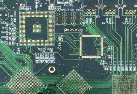
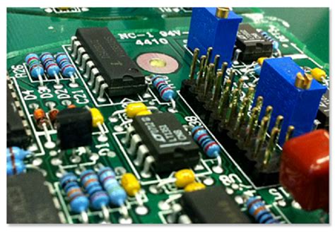
Printed Circuit Boards (PCBs) are the foundation of nearly all modern electronic devices, from smartphones and computers to medical equipment and aerospace systems. As technology advances, the demand for high-precision PCBs has grown exponentially. High-precision PCB manufacturing involves stringent design rules, advanced fabrication techniques, and rigorous quality control to ensure reliability, performance, and miniaturization.
This article explores the key aspects of high-precision PCB manufacturing, including design considerations, materials, fabrication processes, challenges, and applications.
1. The Importance of High-Precision PCBs
High-precision PCBs are essential for applications requiring:
- Miniaturization – Smaller components and finer traces enable compact electronic devices.
- High-Speed Performance – Precise impedance control reduces signal loss in high-frequency circuits.
- Reliability – Tight tolerances ensure consistent performance in harsh environments.
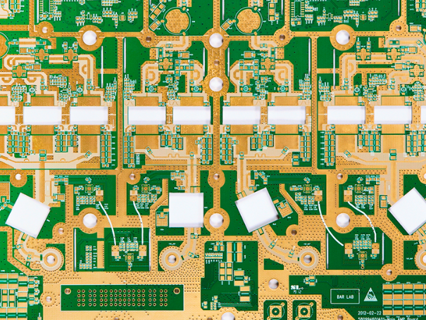
- Complex Multilayer Designs – Advanced PCBs with multiple layers require precise alignment and via formation.
Industries such as aerospace, medical devices, telecommunications, and automotive rely on high-precision PCBs for critical functionalities.
2. Key Design Considerations
2.1 Trace Width and Spacing
High-precision PCBs require extremely fine traces (as small as 2 mil or 50 microns) and tight spacing to accommodate dense circuitry. Designers must account for:
- Impedance Control – Ensuring signal integrity in high-speed designs.
- Current Carrying Capacity – Wider traces for power lines to prevent overheating.
- Manufacturing Capabilities – Aligning designs with fabrication limitations.
2.2 Layer Stackup and Material Selection
Multilayer PCBs (up to 50+ layers in advanced applications) demand careful material selection:
- High-Frequency Materials – Rogers, Teflon, or ceramic-filled laminates for RF/microwave applications.
- Low-Loss Dielectrics – Minimizing signal attenuation in high-speed designs.
- Thermal Management – Metal-core or high-Tg materials for heat dissipation.
2.3 Via Technology
- Microvias (laser-drilled, < 100µm diameter) for HDI (High-Density Interconnect) PCBs.
- Blind and Buried Vias – Used in complex multilayer designs to save space.
- Via-in-Pad – Placing vias directly under components to reduce footprint.
2.4 Surface Finish
The choice of surface finish impacts solderability and signal integrity:
- ENIG (Electroless Nickel Immersion Gold) – Excellent for fine-pitch components.
- OSP (Organic Solderability Preservative) – Cost-effective but less durable.
- Immersion Silver/Tin – Good for high-frequency applications.
- Hard Gold Plating – Used in high-wear environments (e.g., connectors).
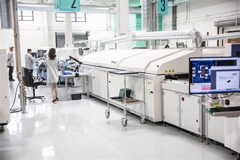
3. Advanced Manufacturing Processes
3.1 Laser Direct Imaging (LDI)
Traditional photolithography uses masks, but LDI employs lasers to directly expose photoresist, enabling finer features (< 20µm resolution).
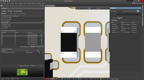
3.2 Automated Optical Inspection (AOI)
AOI systems scan PCBs for defects like shorts, opens, and misalignments with micron-level accuracy.
3.3 Plasma Etching
Used for precise removal of copper and dielectric materials, especially in HDI and flexible PCBs.
3.4 Sequential Lamination
For multilayer PCBs, layers are laminated in stages to ensure proper alignment and via formation.
3.5 Direct Plating
Eliminates the need for chemical deposition, improving via reliability in high-aspect-ratio designs.
4. Challenges in High-Precision PCB Manufacturing
4.1 Tolerances and Yield Rates
Tighter tolerances increase the risk of defects, requiring advanced process control to maintain yield.
4.2 Signal Integrity Issues
Cross-talk, EMI, and impedance mismatches must be minimized through careful design and material selection.
4.3 Thermal Management
High-power and high-frequency designs generate heat, necessitating effective thermal vias and heatsinking.
4.4 Cost vs. Performance Trade-offs
High-precision PCBs are expensive due to specialized materials and processes. Balancing cost and performance is crucial.
5. Applications of High-Precision PCBs
5.1 Medical Devices
- Implantable Electronics – Pacemakers, neurostimulators.
- Diagnostic Equipment – MRI machines, ultrasound systems.
5.2 Aerospace and Defense
- Avionics – Flight control systems, radar.
- Satellite Communications – High-frequency RF PCBs.
5.3 Automotive Electronics
- ADAS (Advanced Driver Assistance Systems) – Lidar, radar PCBs.
- Electric Vehicles (EVs) – Battery management systems.
5.4 Consumer Electronics
- Smartphones & Wearables – Miniaturized, high-density PCBs.
- 5G Technology – Millimeter-wave PCBs for high-speed data.
6. Future Trends
6.1 Additive Manufacturing (3D-Printed PCBs)
Emerging techniques allow for rapid prototyping and complex geometries.
6.2 Embedded Components
Passive and active components integrated within the PCB substrate.
6.3 AI-Driven Design and Inspection
Machine learning optimizes layouts and detects defects faster.
6.4 Flexible and Stretchable PCBs
For wearable and IoT applications.
Conclusion
High-precision PCB manufacturing is a critical enabler of modern electronics, pushing the boundaries of miniaturization, speed, and reliability. As demand grows for smarter, faster, and more compact devices, advancements in materials, fabrication techniques, and quality control will continue to drive innovation in this field.
For industries relying on cutting-edge electronics, partnering with experienced high-precision PCB manufacturers is essential to ensure performance, durability, and compliance with stringent standards.