High-Quality PCB Production: Cost-Effective Reliability

Key Takeaways
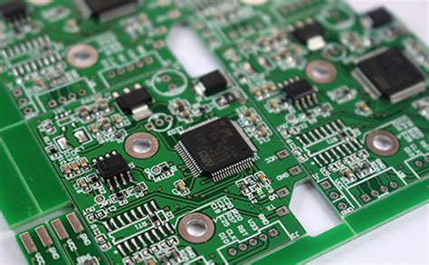
When navigating PCB manufacturing, understanding core value drivers helps optimize both quality and expenses. Leading PCB manufacturing companies leverage automation to enhance precision while controlling PCB manufacturing cost—a critical factor for startups and established firms alike. By implementing advanced inspection systems, these providers minimize defects in high-volume production runs, ensuring your designs meet industry standards without compromising affordability.
Tip: Always verify if your supplier uses AI-powered optical inspection—this technology typically reduces error rates by 40-60% compared to manual checks.
Your choice of partner significantly impacts the PCB manufacturing business outcomes. Look for providers offering transparent breakdowns of material costs, layer complexity fees, and testing surcharges. For instance, industry leaders combine automated defect detection with real-time yield analytics, allowing you to identify cost-saving opportunities early in prototyping phases. This approach not only accelerates time-to-market but also prevents costly revisions in later stages.
Transitioning from design to production? Prioritize vendors providing dual-track support: scalable solutions for bulk orders and flexible low-volume options for iterative testing. This strategy ensures you maintain reliability across small batches and large-scale deployments while keeping per-unit expenses predictable.

Automating PCB Quality Control Processes
When managing PCB manufacturing costs and timelines, automating quality control (QC) processes ensures consistency while reducing human error. Modern PCB manufacturing companies leverage advanced systems like automated optical inspection (AOI) and X-ray inspection to detect microscopic defects—from soldering flaws to trace misalignments—that manual checks might overlook. These technologies scan boards at high speeds, comparing designs against production outputs with sub-millimeter precision, which is critical for maintaining reliability in high-density circuits.
For businesses balancing PCB manufacturing business scalability with quality, integrating automated QC minimizes rework expenses and accelerates time-to-market. For instance, AOI systems flag issues early, allowing real-time corrections during assembly. Similarly, automated electrical testing validates functionality before shipment, reducing field failures. By adopting these tools, you not only lower long-term PCB manufacturing cost risks but also align with industry standards for durability—a necessity for applications in aerospace, medical devices, or IoT systems.
Transitioning to automated workflows doesn’t eliminate human expertise but refocuses it on optimizing design validation and process improvements. This shift ensures your projects benefit from both precision engineering and cost-effective scalability, setting the stage for exploring strategies that further harmonize affordability with performance.
Cost-Effective PCB Manufacturing Strategies
When optimizing PCB manufacturing processes, balancing efficiency and quality requires strategic planning. Leading PCB manufacturing companies achieve cost reductions through economies of scale by standardizing designs and bulk-ordering materials. For instance, consolidating orders for FR-4 substrates or surface finishes like HASL minimizes PCB manufacturing cost while maintaining performance. You can further lower expenses by partnering with suppliers offering volume discounts or recycled copper-clad laminates without compromising durability.
Automation plays a pivotal role in cost management. Advanced pick-and-place systems and automated optical inspection (AOI) reduce labor-intensive tasks, slashing error rates by up to 70% in high-volume runs. This approach not only accelerates production but also ensures consistency—a critical factor for startups scaling their PCB manufacturing business. Additionally, modular design practices allow reusing validated circuit blocks across projects, trimming development time and material waste.
However, affordability shouldn’t overshadow reliability. Implementing design-for-manufacturability (DFM) checks early in the process helps avoid costly revisions. Many manufacturers now integrate real-time analytics to monitor yield rates, enabling proactive adjustments to material usage or layer stacking. By aligning these strategies, you maintain competitive PCB manufacturing cost thresholds while delivering boards that meet industrial-grade standards—a foundation for the subsequent discussion on quality assurance protocols.

JLCPCB Quality Assurance Protocols Explained
When selecting PCB manufacturing companies, understanding their quality control frameworks directly impacts your project’s success. JLCPCB employs a multi-layered inspection system designed to minimize errors while optimizing PCB manufacturing cost. Their protocols begin with automated optical inspection (AOI), which scans for soldering defects and misalignments at micron-level precision. This step ensures traceability across batches, a critical factor for scaling PCB manufacturing business operations.
For high-density designs, JLCPCB integrates X-ray testing to examine inner-layer connections—essential for avoiding latent failures in complex boards. Their material verification process includes thermal stress tests, ensuring substrates withstand operating temperatures without delamination.
| QA Stage | Key Function | Impact on Reliability |
|---|---|---|
| AOI Scanning | Detects surface defects | Reduces assembly rework by 40%+ |
| X-ray Inspection | Validates internal via integrity | Prevents 95% of hidden faults |
| Material Testing | Certifies substrate durability | Extends product lifespan by 30% |
By aligning these protocols with ISO 9001 standards, JLCPCB balances cost-efficiency and consistency—a priority for businesses managing tight PCB manufacturing budgets. Their real-time reporting portal lets you monitor quality metrics, ensuring transparency from prototype to mass production. This approach not only mitigates risks but also streamlines timelines, making it easier to meet demanding project deadlines without compromising durability.

Precision Engineering for Reliable Circuit Boards
Achieving reliability in PCB manufacturing begins with precision engineering—a meticulous approach that ensures every layer, trace, and component aligns with exacting standards. Modern PCB manufacturing companies leverage advanced design software to simulate electrical performance, thermal behavior, and signal integrity before production begins. This proactive engineering minimizes risks like impedance mismatches or heat buildup, which could compromise durability.
To balance PCB manufacturing cost with quality, engineers optimize material selection—using high-Tg laminates for thermal stability or controlled-impedance substrates for high-frequency applications. Automated routing algorithms further refine designs, reducing signal loss while maximizing board space efficiency. These steps ensure that even budget-conscious projects don’t sacrifice long-term reliability.
For PCB manufacturing business models prioritizing scalability, precision extends to process control. Laser-drilled vias, solder mask application with ±0.05mm accuracy, and automated optical inspection (AOI) systems guarantee consistency across batches. By integrating these technologies, manufacturers deliver boards that withstand harsh environments—whether in consumer electronics or industrial machinery—without inflating costs.
Ultimately, precision engineering bridges the gap between affordability and performance, ensuring your circuit boards meet both functional demands and lifecycle expectations.
Balancing Affordability and PCB Durability
When navigating PCB manufacturing, achieving the right balance between cost and durability often feels like walking a tightrope. While cutting PCB manufacturing costs might seem tempting, compromising on material quality or production standards can lead to premature failures, costing more in repairs or replacements. Leading PCB manufacturing companies address this by optimizing design choices—like selecting cost-effective substrates without sacrificing thermal stability—and leveraging economies of scale. For instance, high-volume production runs reduce per-unit expenses, allowing you to invest in advanced surface finishes that enhance corrosion resistance.
The PCB manufacturing business thrives on precision, but affordability doesn’t have to mean cutting corners. Modern techniques, such as automated panelization, minimize material waste, while rigorous testing protocols—like impedance control and thermal stress tests—ensure reliability without inflating budgets. Partnering with manufacturers that offer tiered pricing models lets you align expenses with project complexity. For example, opting for standard FR-4 substrates for non-critical layers while reserving high-performance materials for power-heavy sections maintains durability without overspending.
Ultimately, the key lies in transparent communication with your manufacturer. Clarify your performance requirements and budget constraints upfront to unlock tailored solutions that deliver both long-term reliability and cost efficiency. By prioritizing value over the lowest upfront price, you secure circuit boards that withstand real-world demands without straining resources.
Defect Detection in Modern PCB Production
When managing PCB manufacturing costs, you need solutions that prevent expensive rework without compromising quality. Modern PCB manufacturing companies leverage automated optical inspection (AOI) and X-ray imaging to identify micron-level defects like solder bridges, misaligned components, or micro-cracks. These systems scan boards at speeds exceeding human capability, flagging inconsistencies in real time while maintaining throughput. For instance, automated defect detection reduces human error risks by 60–80%, directly lowering long-term PCB manufacturing business expenses tied to warranty claims or recalls.
Advanced algorithms in AOI systems compare designs against production outputs, detecting deviations as small as 10μm. This precision ensures even high-density boards meet IPC-A-600 standards before final testing. Some manufacturers integrate machine learning to refine inspection accuracy over time, adapting to new design complexities. By prioritizing these technologies, you ensure reliability without inflating PCB manufacturing budgets—critical for balancing affordability and performance. Transitioning to automated workflows also minimizes manual checks, freeing resources for innovation or scaling operations.
For DIY projects or low-volume batches, partnering with firms offering real-time defect analytics ensures your prototypes match production-grade quality. This approach future-proofs your designs, whether you’re iterating quickly or preparing for mass production.
Expert Assembly Support for DIY PCB Projects
Navigating PCB manufacturing for DIY projects often requires balancing technical precision with budget constraints. While assembling boards yourself can reduce PCB manufacturing cost, even minor errors in solder paste application or component placement may compromise reliability. This is where partnering with PCB manufacturing companies offering expert assembly support becomes invaluable. Many providers now integrate guided design reviews and troubleshooting assistance, ensuring your prototype aligns with industry-grade standards without overcomplicating the process.
For instance, leading firms provide step-by-step guidance on optimizing layouts for automated assembly, helping you avoid common pitfalls like tombstoning or cold joints. Such support not only streamlines production but also minimizes rework expenses—a critical factor when scaling from prototypes to small batches. What many overlook is how these services democratize access to professional-grade outcomes, bridging the gap between hobbyist experimentation and commercial viability in the PCB manufacturing business.
By leveraging these resources, you gain access to advanced techniques like selective soldering or BGA reballing, which are typically reserved for high-volume production. This becomes particularly valuable when transitioning from DIY projects to market-ready products, ensuring your design maintains durability while staying cost-efficient.
PCBWay’s Automated Inspection Technologies
When optimizing PCB manufacturing workflows, automated inspection systems play a pivotal role in balancing speed and accuracy. PCBWay integrates advanced technologies like automated optical inspection (AOI) and X-ray inspection to identify defects such as solder bridging, misaligned components, or trace fractures at micron-level precision. By implementing these systems, PCB manufacturing companies can reduce human error while scaling production—critical for maintaining competitive PCB manufacturing cost structures.
These technologies work in tandem with AI-powered analytics to classify defects in real time, allowing engineers to address issues before they escalate. For instance, AOI systems scan thousands of solder joints per minute, cross-referencing results against design specifications to ensure compliance. This approach not only safeguards product reliability but also minimizes material waste—a key consideration for any PCB manufacturing business aiming to improve margins without compromising quality.
Transitioning from manual checks to automated processes also streamlines quality assurance timelines, enabling faster turnaround for complex multilayer boards. Whether you’re prototyping or scaling up production, integrating such systems ensures consistent output—a necessity in industries where even minor flaws can lead to costly failures. By prioritizing defect prevention over post-production fixes, manufacturers can deliver durable circuit boards that align with both technical and budgetary expectations.
Conclusion
When navigating the complexities of PCB manufacturing, striking the right balance between PCB manufacturing cost and reliability requires careful planning. Leading PCB manufacturing companies leverage advanced automation and precision engineering to minimize defects while maintaining affordability. By adopting rigorous quality protocols, such as automated optical inspection (AOI) and real-time performance testing, these firms ensure that durability doesn’t come at the expense of budget constraints.
For your PCB manufacturing business or DIY projects, partnering with providers that integrate expert assembly support with cutting-edge defect detection systems can streamline production timelines and reduce long-term risks. Whether prioritizing cost-efficiency or mission-critical performance, modern solutions empower you to scale operations without compromising on quality. As you evaluate options, consider how innovative technologies and transparent pricing models align with your specific needs—ensuring every circuit board delivers consistent, dependable results.
FAQs
How do PCB manufacturing companies ensure reliability without inflating costs?
Leading PCB manufacturing firms optimize PCB manufacturing cost through automated defect detection and standardized testing protocols. By integrating precision engineering with bulk production efficiencies, they maintain affordability while meeting industry durability benchmarks.
What factors most impact PCB manufacturing cost for small businesses?
Material selection, layer count, and turnaround time are primary cost drivers. Reputable PCB manufacturing businesses offer tiered pricing models, allowing you to scale orders while preserving quality. Advanced panelization techniques further reduce waste in high-volume runs.
Can PCB manufacturing processes accommodate custom design requirements?
Yes, most professional PCB manufacturing companies provide design-for-manufacturing (DFM) analysis. This service identifies potential production issues before fabrication, ensuring your specialized layouts align with PCB manufacturing capabilities while avoiding costly revisions.
How do I verify a PCB manufacturing business meets quality standards?
Request certifications like ISO 9001 and IPC Class 2/3 compliance reports. Top-tier providers transparently share their inspection methodologies, including AOI (Automated Optical Inspection) logs and impedance control documentation for high-frequency boards.
Ready to Optimize Your PCB Project?
For tailored solutions that balance PCB manufacturing cost with uncompromised reliability, please click here to explore advanced fabrication options. Technical support teams are available to review your design specifications and recommend cost-efficient production strategies.