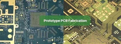
High-Quality PCB Prototypes: Expert Manufacturing Techniques
Key Takeaways
When navigating PCB manufacturing for prototypes, understanding critical factors ensures you avoid costly pitfalls. First, laser-cut SMT integration minimizes alignment errors, enabling precise component placement—a must for high-frequency or miniaturized designs. Leading PCB manufacturing companies leverage multi-panel optimization to reduce PCB manufacturing cost by up to 30%, grouping multiple designs into a single panel without compromising quality.
For time-sensitive projects, 24-hour rapid build techniques combine automated routing with real-time design validation, slashing lead times while maintaining reliability. Rigorous thermal cycling and signal integrity testing validate durability, ensuring prototypes withstand real-world conditions before scaling production.
| Cost Factor | Traditional Approach | Optimized Strategy |
|---|---|---|
| Material Usage | Single-panel | Combined panels |
| Assembly Time | Manual adjustments | Automated SMT integration |
| Testing Overhead | Post-build checks | In-process validation |
Balancing PCB manufacturing business priorities—speed, accuracy, and affordability—requires adopting low-volume assembly solutions. These streamline workflows for complex designs, such as HDI or mixed-signal boards, while avoiding overstock risks. By integrating streamlined ordering systems, you gain visibility into material availability and pricing tiers, enabling smarter budgeting without sacrificing technical requirements.
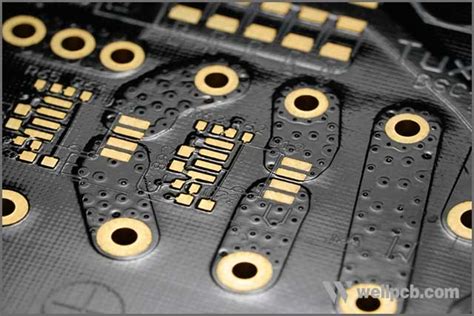
Laser SMT Integration in PCB Prototyping
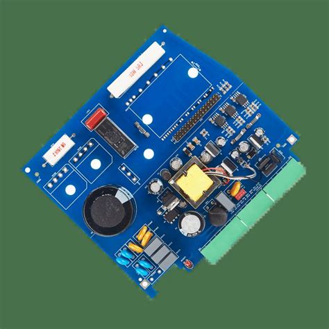
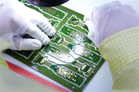
When creating high-quality PCB prototypes, integrating laser-cut surface-mount technology (SMT) ensures unmatched precision for complex designs. Modern PCB manufacturing companies leverage femtosecond lasers to achieve micron-level accuracy in drilling microvias and trimming components, reducing errors that traditional mechanical methods might introduce. This approach minimizes PCB manufacturing cost by eliminating tooling wear and material waste, particularly beneficial for low-volume runs.
Tip: Always verify that your prototyping partner uses automated optical inspection (AOI) alongside laser SMT systems to catch defects early, saving time and resources.
By combining laser alignment with advanced pick-and-place systems, you gain tighter control over component placement—critical for high-density interconnects or RF applications. This integration also accelerates turnaround times, a key advantage when balancing speed and quality in the PCB manufacturing business. For optimal results, collaborate with manufacturers who offer transparent process documentation to track every stage of your prototype’s development.
Transitioning to laser-driven processes future-proofs your designs, ensuring compatibility with emerging standards like 5G or IoT devices. As you refine your requirements, this method seamlessly aligns with subsequent steps in multi-panel optimization, further enhancing cost efficiency.
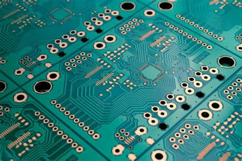
Multi-Panel Optimization for Cost Efficiency
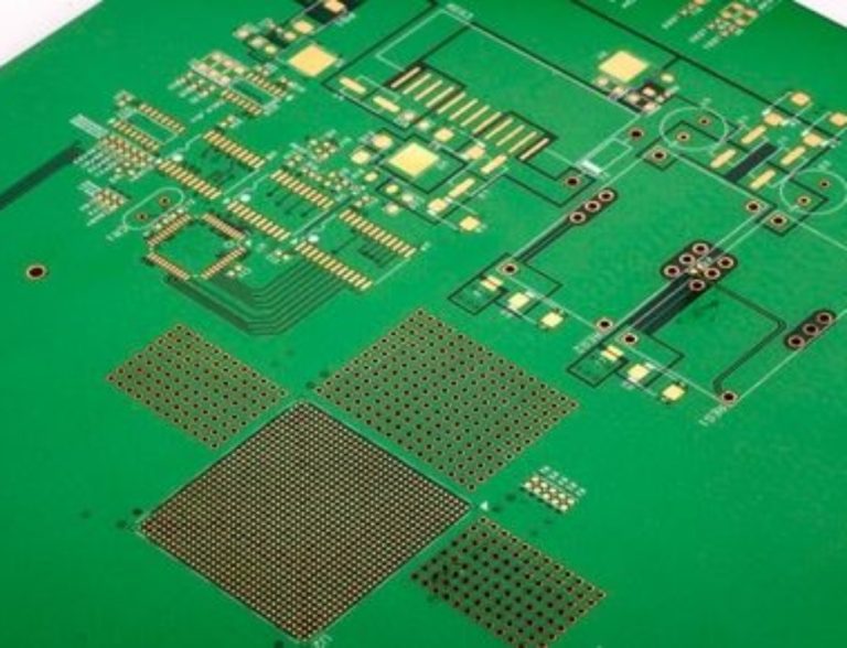
When ordering PCB manufacturing services, optimizing panel layouts directly impacts your project’s affordability. By arranging multiple circuit designs on a single production panel, PCB manufacturing companies minimize material waste and streamline fabrication processes. This approach reduces the pcb manufacturing cost per unit, particularly for low-volume orders, while maintaining precision across all designs.
Advanced software tools analyze panel utilization rates, ensuring maximum space efficiency without compromising trace integrity. For example, grouping designs with similar layer counts or thicknesses can boost panel yield by 15–30%, translating to measurable savings. However, balancing density with accessibility for testing and assembly remains critical—overcrowding panels risks defects that negate initial savings.
Collaborating with experienced pcb manufacturing business partners ensures tailored solutions. They’ll guide you in selecting standardized panel sizes or combining orders with other projects to further reduce material costs. This strategy not only lowers expenses but also aligns with sustainable practices by minimizing scrap.
By prioritizing multi-panel optimization, you transform upfront pcb manufacturing cost investments into long-term value—a vital consideration for scaling prototypes into production-ready designs.
24-Hour Rapid PCB Build Techniques
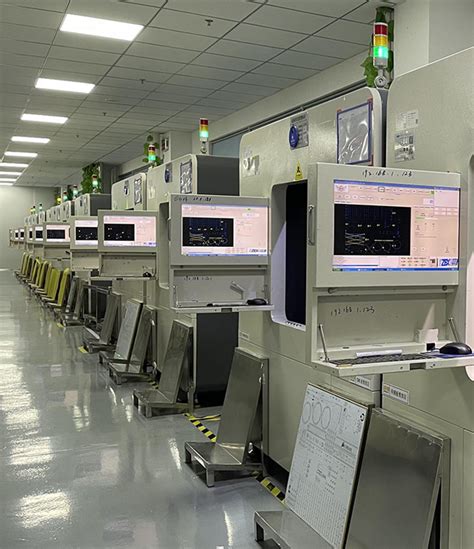
When time is critical, PCB manufacturing companies leverage automated workflows and precision machinery to deliver prototypes within 24 hours. By integrating laser-cut SMT integration with advanced pick-and-place systems, these providers minimize manual intervention, accelerating assembly without compromising accuracy. Automated optical inspection (AOI) systems further streamline quality checks, ensuring defects are flagged in real time.
To meet tight deadlines, prioritize PCB manufacturing partners that employ panelization strategies, grouping multiple designs onto a single board to optimize material use and reduce PCB manufacturing cost. This approach aligns with multi-panel optimization principles, enabling faster batch processing while maintaining design integrity. For complex layouts, automated routing software adjusts trace widths and spacing dynamically, avoiding bottlenecks during fabrication.
Rapid builds also depend on pre-validated component libraries and design-for-manufacturability (DFM) checks, which identify potential issues before production begins. By collaborating with PCB manufacturing business experts early, you avoid costly redesigns and ensure files meet technical specifications. Additionally, modular tooling setups allow manufacturers to switch between projects swiftly, supporting low-volume runs without excessive downtime.
While speed is prioritized, reliability remains non-negotiable. Reputable providers pair accelerated timelines with rigorous testing protocols, such as in-line electrical testing, to validate functionality before shipment. This balance ensures your prototype not only arrives quickly but performs as intended in real-world applications.
Reliability Testing for Prototype Durability
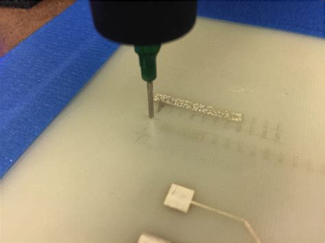
After perfecting your design through PCB manufacturing techniques like laser-cut SMT integration, validating durability becomes critical. Leading PCB manufacturing companies implement thermal cycling and signal integrity analysis to simulate real-world stressors, ensuring prototypes withstand extreme temperatures, voltage fluctuations, and mechanical strain. These tests identify weaknesses in solder joints, material expansion, or trace alignment—issues that could escalate PCB manufacturing cost if unaddressed during mass production.
For low-volume builds, accelerated life testing (ALT) combines humidity chambers and vibration tables to replicate years of operation in days. This step is vital for high-frequency or IoT applications, where even minor flaws compromise performance. Advanced firms also use automated optical inspection (AOI) to scan for micro-cracks or misaligned components, reducing human error in quality checks.
While rigorous testing adds upfront time, it prevents costly redesigns and strengthens client trust in your PCB manufacturing business. By prioritizing reliability early, you ensure prototypes meet not just functional specs but long-term operational demands—balancing precision with cost-efficiency for complex designs.
Low-Volume PCB Assembly Cost Solutions
When managing PCB manufacturing expenses for small batches, strategic planning ensures you avoid overspending without compromising quality. Material selection plays a critical role—opting for standardized substrates and finishes reduces PCB manufacturing cost while maintaining performance. Partnering with PCB manufacturing companies that specialize in low-volume orders allows you to leverage economies of scale through shared panelization, where multiple designs are grouped on a single production panel. This approach minimizes material waste and lowers per-unit pricing.
Advanced PCB manufacturing business practices, such as automated assembly lines, further cut labor costs. By integrating surface-mount technology (SMT) for high-density components, you reduce manual soldering requirements, accelerating turnaround times. Additionally, modular design principles—like reusing validated circuit blocks—streamline assembly and testing phases, preventing costly redesigns.
To optimize budgets, prioritize suppliers offering transparent pricing models for prototypes. Many providers now offer tiered pricing based on order frequency, rewarding repeat clients with incremental discounts. Combining these strategies with just-in-time inventory management ensures you only pay for what you need, avoiding excess stockpiling. Ultimately, balancing cost-efficiency with technical precision ensures your low-volume projects remain viable and competitive.
Advanced Techniques for Complex PCB Designs
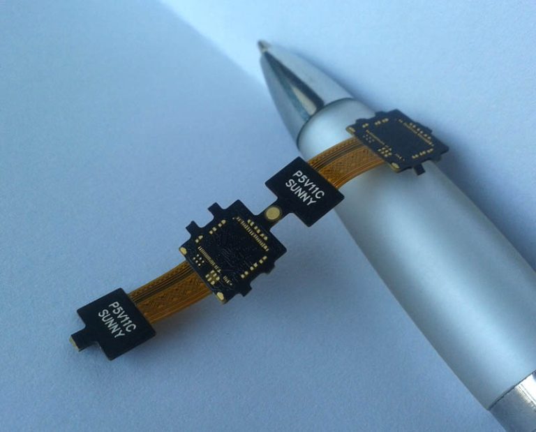
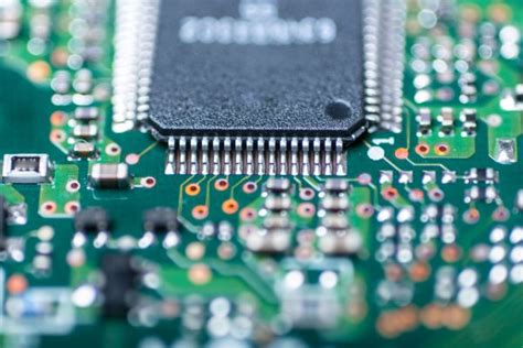
When tackling intricate layouts like high-density interconnect (HDI) substrates or flex-rigid boards, PCB manufacturing companies rely on specialized strategies to balance performance and feasibility. For designs requiring ultra-fine traces (below 3 mil), laser direct imaging (LDI) systems enable precise pattern transfers, minimizing signal loss in high-frequency applications. Advanced PCB manufacturing workflows also integrate embedded component technology, allowing passive elements like resistors or capacitors to be buried within layer stacks—freeing surface space for critical active components.
To address PCB manufacturing cost challenges in complex projects, engineers use dynamic panelization to nest multiple designs into a single fabrication panel. This approach, combined with automated optical shaping (AOS), reduces material waste by up to 22% compared to traditional methods. For designs with mixed-signal requirements, PCB manufacturing business experts recommend controlled impedance routing paired with 3D electromagnetic simulation tools to pre-validate signal integrity before prototyping.
When working with PCB manufacturing partners, ensure they employ sequential lamination for multilayer builds exceeding 16 layers. This technique prevents delamination risks in high-temperature environments while maintaining consistent dielectric properties across layers. By aligning your design rules with design-for-manufacturability (DFM) guidelines early, you avoid costly revisions and accelerate time-to-market for even the most sophisticated boards.
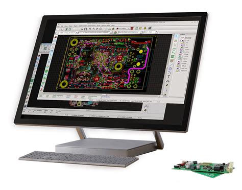
Streamlined PCB Prototyping Ordering Systems
Modern PCB manufacturing companies leverage digital platforms to simplify the ordering process, ensuring speed and precision for complex projects. By integrating automated quote generators and real-time design verification tools, these systems eliminate manual errors while reducing PCB manufacturing cost through optimized material usage. You can upload design files directly to cloud-based portals, where algorithms instantly flag potential issues like spacing violations or impedance mismatches—critical for maintaining design accuracy before production begins.
Advanced platforms also enable live tracking of your prototype’s progress, from fabrication to assembly, minimizing communication gaps with suppliers. For PCB manufacturing business clients managing multiple iterations, batch ordering features allow simultaneous processing of design variants, cutting turnaround times by up to 40%. Automated panelization tools further streamline workflows by grouping designs into combined layouts, maximizing material efficiency without compromising quality.
To stay competitive, prioritize providers offering API integrations with popular CAD software, ensuring seamless data transfer between your engineering team and their PCB manufacturing lines. This approach not only accelerates prototyping cycles but also scales effortlessly for low-volume production runs, aligning cost structures with project demands.
Combined Panel Orders for Material Savings
When optimizing PCB manufacturing costs, combining multiple designs into a single panel proves indispensable. By grouping smaller boards within standardized panel sizes, PCB manufacturing companies minimize material waste—a critical factor in reducing per-unit expenses. This approach leverages economies of scale, allowing you to share base materials like FR-4 or Rogers substrates across multiple prototypes. Advanced PCB manufacturing business practices often employ automated nesting software to arrange designs with precision, ensuring maximum utilization of copper-clad laminates while maintaining required spacing for routing and depaneling.
For low-volume orders, this strategy directly impacts your PCB manufacturing budget. Instead of dedicating entire panels to a single design, combining projects lowers raw material consumption by up to 30%, depending on board geometry. However, collaboration with your manufacturer is key—confirm their panelization guidelines to avoid conflicts with tooling holes or fiducial markers. Leading providers also offer mixed-panel options, enabling you to prototype varied designs simultaneously without compromising turnaround times. By aligning your panel strategy with production workflows, you achieve cost efficiency while preserving the integrity of complex layouts—a balance that defines modern PCB manufacturing excellence.
Conclusion
When navigating PCB manufacturing for prototype development, selecting the right partner becomes critical to balancing precision, speed, and affordability. Leading PCB manufacturing companies leverage advanced processes like laser-cut SMT integration and multi-panel optimization to reduce PCB manufacturing cost while maintaining rigorous quality standards. These techniques not only accelerate turnaround times but also ensure your prototypes meet functional requirements for complex designs.
By aligning with experienced providers, you gain access to cost-efficient low-volume solutions that minimize material waste without sacrificing reliability—key for iterative testing. Whether you’re optimizing PCB manufacturing business workflows or scaling production, prioritizing traceability and data-driven testing protocols ensures long-term durability. Transparent communication during ordering further streamlines collaboration, helping you avoid delays and unexpected expenses.
Ultimately, the success of your project hinges on choosing partners who understand the interplay between technical precision and economic viability. By focusing on these principles, you position yourself to prototype with confidence, knowing every layer of your design aligns with both performance goals and budget constraints.
FAQs
How do pcb manufacturing companies ensure precision in prototypes?
They employ advanced laser-cut SMT integration and automated optical inspection (AOI) systems to maintain micron-level accuracy, critical for complex designs.
What factors influence pcb manufacturing cost for low-volume orders?
Material selection, layer count, and panelization strategies directly affect pricing. Multi-panel optimization reduces waste, lowering expenses without compromising quality.
Can pcb manufacturing timelines align with urgent project needs?
Yes, streamlined workflows and 24-hour rapid builds enable fast-turnaround prototypes, ideal for iterative testing or time-sensitive product launches.
How is reliability tested in pcb manufacturing business operations?
Prototypes undergo thermal cycling, impedance testing, and functional validation to ensure durability under real-world operating conditions.
What design complexities challenge pcb manufacturing companies?
High-density interconnects (HDI), mixed-signal layouts, and RF components require specialized laser-drilled microvias and impedance-controlled routing expertise.
Ready to Start Your Project?
For tailored solutions that balance pcb manufacturing cost and performance, click here to explore our services. Our team optimizes every stage, from design review to final testing.