High-Speed Interconnect Requirements Drive Cheaper PCB Materials
When reading and researching articles and the plethora of opinions on the internet, it’s easy to assume that the consensus among the informed is that the days of using traditional low-cost PCB materials for next-generation high-speed designs are long gone. There’s also a view that the requirements of modern technologies, such as PCIe 5.0 and beyond, have pushed the boundaries of circuit board design and manufacturing to the edge.
However, a closer look at the materials and methods involved offers new hope that while we are indeed sprinting ever closer to the edge, there are some key adjustments we can make that might allow us to stop crossing it, at least for now.
Cost of Next-Generation PCB Materials
While it’s true that using next-generation materials makes it easier to incorporate new technologies into designs, this increase in capability and performance comes at a real cost: it’s much more expensive to manufacture PCBs using exotic materials. Depending on the design details, the increase could be in the 100% (2x) or even more.
Some companies prefer to make this giant leap because their systems and designs can accommodate the use of exotic materials and absorb the additional costs associated with their use. However, there are many others who are subject to tighter design and budget constraints that will make the transition more difficult.
For this reason, Intel engineers have been hard at work examining the various factors involved and providing multiple approaches that will enable designers to build next-generation technologies into their designs using lower-cost current PCB materials and processes.

Cost is not the only consideration
Some increase in manufacturing costs is inevitable when incorporating next-generation technologies into your designs. However, our research has determined that it is possible to keep the increase within 30% through a variety of variables.
Below are some of the more easily applied insights gleaned from the research we conducted. However, as you read, it is important to remember that this approach is not a panacea—there are trade-offs at every level, and while overall cost is important, it is only one of the factors that must be considered.
Design variables
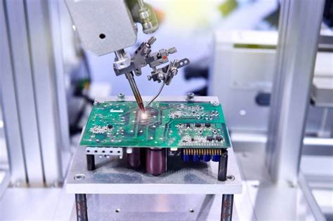
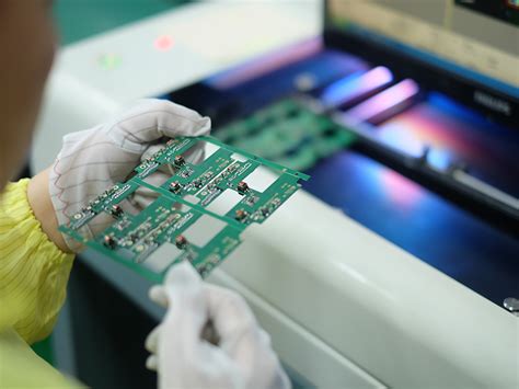
When manufacturing PCBs, many variables must be considered. However, our efforts have determined that the greatest benefits come from focusing specifically on four of these design variables: dielectric material, copper surface roughness, oxidation process, and optimization of the stackup. For each design variable, we have also listed options that the industry can invest in and provide cost-effective solutions.
1.Dielectric Materials
Traditional FR4 dielectric materials use epoxy-based resins and E-glass reinforcement systems to reduce costs. Specialty dielectric materials often require the use of more expensive PPE/PPO-based resin systems and/or low D k glass for better performance, increasing overall manufacturing costs.
Option: Newer production methods have been developed that combine epoxy with PPE/PPO-based resins, resulting in finished boards with performance characteristics that meet performance requirements but are less expensive to manufacture.
2.Surface Roughness of Copper
Ideally, high-speed signals would pass through paths made of copper with no surface roughness. Unfortunately, in the real world, using “smooth” copper is impossible because other materials have a hard time adhering to it and the PCB would delaminate and fall apart. Therefore, all copper used in PCB manufacturing has some degree of roughness. For boards with higher electrical performance and lower loss requirements, manufacturers use copper with a lower (smoother) profile. The downside is that these materials are more expensive.
Option: Using a new type of copper foil, commonly called RTF2, is becoming more popular in the market. RTF2 is a copper foil with a non-uniform roughness profile that performs close to that of high-very-thin-profile (HVLP) copper foil, but can be manufactured at a lower cost. Next-generation RTF2 copper foils are also being investigated to achieve HVLP-like performance while minimizing the cost increase.
3.Oxidation Process
In PCB manufacturing, a surface oxidation process is often required to promote adhesion between the core layer and the prepreg layer for optimal bonding. A precise balance must be achieved in this process because while increasing the surface roughness of the copper foil will help improve adhesion, it can have a significant negative impact on the copper profile, which can affect signal integrity. An imprecise or unnecessarily aggressive oxidation process can offset the improvements obtained by over-roughening the copper foil before bonding.
Options: The industry is developing and adopting low-etch oxidation chemistries and adhesion promoters – they can reduce the copper surface roughening requirements while maintaining the bond strength required for PCBs. Less surface oxidation also reduces the potential negative impact on signal integrity, making this approach a win-win.

4.Stackup Optimization
In some ways, correctly determining the PCB stackup is low-hanging fruit in the process of performance optimization and cost minimization, as thickness matters.
Options: When looking closely at the signal loss characteristics of the more common core/prepreg layer thickness options, it becomes clear that losses can be minimized simply by taking the time to determine the correct stackup. In a test conducted by Intel engineers, it was found that when measuring signal loss, a 5/6 stackup (5 mil core thickness and 6 mil prepreg thickness) performed more than 15% better than a 3/9 stackup using the same substrate and copper profiles.
Of course, this approach is not a slam dunk, as changes in the stackup can negatively impact routing density and noise coupling. However, it does highlight that careful selection of the stackup and its signal integrity impact is a critical step in the process of performance and cost optimization.
Working with Academia
As mentioned above, Intel has undertaken this research effort to provide alternatives for companies that may find it difficult or even impossible to build next-generation materials into their systems and designs. But even with the vast resources at Intel’s disposal, there are gaps in R&D that we simply cannot fill alone.
Therefore, academia must be involved in these efforts at every level. Several advances in this area have been made by industry experts and academicians, who share the common goal of identifying, studying, and solving the problems that plague PCB manufacturing. This collaborative approach is key to ensuring that our industry continues to innovate and grow for many years to come, just as it is today.