High-speed PCB crosstalk analysis and minimization
1.Introduction
With the increasing complexity and performance of electronic products, the density of printed circuit boards and the frequency of related devices are constantly rising. Maintaining and improving the speed and performance of the system has become an important issue for designers. The higher the signal frequency, the steeper the edge, the smaller the size of the printed circuit board, and the increased wiring density have significantly increased the impact of crosstalk in high-speed PCB design. The crosstalk problem exists objectively, but exceeding a certain limit may cause false triggering of the circuit, resulting in the system not being able to work properly. Designers must understand the mechanism of crosstalk generation and apply appropriate methods in the design to minimize the negative impact of crosstalk.
2.Generation and change trend of high-frequency digital signal crosstalk
Crosstalk refers to the undesired noise voltage signal generated by the mutual coupling of electromagnetic fields between adjacent signals when the signal propagates on the transmission line, that is, the energy is coupled from one line to another line.
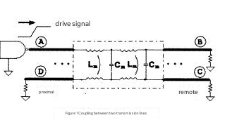
As shown in Figure 1, for the convenience of analysis, we describe the crosstalk model of two adjacent transmission lines according to the discrete equivalent model. The characteristic impedance of transmission lines AB and CD is Z0, and the terminal matching resistance R=Z0. If the driving source at point A is the interference source, the line network between A and B is called the aggressor line, the line network between C and D is called the victim line, the crosstalk of the victim network close to the driving end of the aggressor network is called near-end crosstalk (also called backward crosstalk), and the crosstalk close to the receiving end of the aggressor network is called far-end crosstalk (also called forward crosstalk). Crosstalk mainly comes from the mutual inductance Lm and mutual capacitance Cm formed between two adjacent conductors.
2.1 Inductive coupling
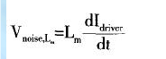
In Figure 1, only the inductive coupling caused by mutual inductance Lm is considered. The magnetic field of the signal transmitted on line A to B induces a voltage on line C to D. The role of magnetic coupling is similar to that of a transformer. Since this is a distributed transmission line, the mutual inductance also becomes a series of transformers distributed on two adjacent parallel transmission lines. When a voltage step signal moves from A to B, each transformer distributed on the interference line will sequentially induce an interference spike pulse to appear on the victim network. The voltage noise superimposed by mutual inductance on the interfered network is proportional to the change of driving current on the interfering network. The noise calculation formula generated by mutual inductance is
It is worth noting that the polarity of mutual inductance coupling in each section of the coupling transformer is different. These interference energies sensed to the interfered network are forward and backward in sequence, but with opposite polarities, and travel along the transmission line CD to points C and D respectively.
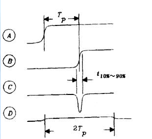
As shown in Figure 2, the forward interference energy in the direction of C is proportional to the incident voltage and each mutual inductance component Lm. Because all the forward interference energy arrives at point C almost at the same time, the forward interference energy is proportional to the total mutual inductance of the two transmission lines. The longer the parallel length of the transmission line, the greater the total mutual inductance generated, and the forward interference energy also increases immediately; however, the backward interference energy to point D is different from the forward interference energy to point C. Although the total area of the two couplings is the same, the interference component induced by each mutual inductance transformer arrives at D in sequence, and the effective time of the backward interference energy is as long as 2Tp (Tp is the propagation delay). As the parallel length of the line increases (i.e. the mutual inductance increases), the amplitude of the backward crosstalk will not change, but the duration will increase.
2.2 Capacitive coupling
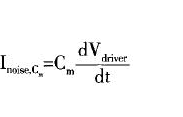
Mutual capacitance is another mechanism for generating crosstalk. Mutual capacitance Cm will generate an induced current in the interfered network, which is proportional to the rate of change of the voltage on the interfered network. The noise calculation formula generated by mutual capacitance Cm is:
The coupling mechanism of distributed coupling capacitance is similar to that of distributed inductive coupling, except for the polarity of the coupling. As shown in Figure 3, the polarities of the forward and backward interference energies of mutual capacitance coupling are both positive.
2.3 Synthetic effect of mutual inductance and mutual capacitance
Usually, capacitive crosstalk and inductive crosstalk occur simultaneously. From the literature [1], we can obtain the calculation formulas for the total crosstalk at the near end and far end, which are respectively formed by the superposition of capacitive coupling and inductive coupling.
The total noise of near-end crosstalk is:
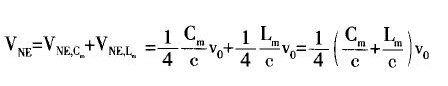
The total noise of far-end crosstalk is:
Wherein, Z0, C, l, Cm, Lm, L, V0 are the characteristic impedance, unit length capacitance, unit length inductance of the transmission line, the coupling capacitance and coupling inductance between the two transmission lines, the parallel length of the two transmission lines and the voltage peak value.
From the above two equations, we can see that the total noise of far-end crosstalk is mutually reduced due to the polarity relationship between capacitive and inductive coupling, that is, far-end crosstalk can be eliminated. In PCB wiring, stripline circuits can better show a good balance between inductive and capacitive coupling, and their forward coupling energy is extremely small; while for microstrip lines, most of the electric field related to crosstalk passes through the air, not other insulating materials, so capacitive crosstalk is smaller than inductive crosstalk, resulting in its forward coupling being a small negative number. This is why in common designs, far-end crosstalk interference is often ignored, and near-end crosstalk improvement is more focused.
In actual design, relevant parameters of PCB (such as thickness, dielectric constant, etc.) as well as line length, line width, line spacing, the position of transmission line and ground plane, and current flow direction will affect the size of c, l, Cm, Lm, L, while the signal frequency and the rise/fall time of the device determine .
Here we do not make a quantitative analysis of the effects of these parameters on crosstalk. For details on the relationship between these parameters and the degree of their effects on crosstalk, please refer to other relevant references.
2.4 Trend of crosstalk
The size of mutual inductance and mutual capacitance affects the size of crosstalk, thereby equivalently changing the characteristic impedance and propagation speed of the transmission line. Similarly, the geometry of the transmission line greatly affects the changes in mutual inductance and mutual capacitance, so the characteristic impedance of the transmission line itself also affects these parameters. In the same medium, the coupling between a relatively low-impedance transmission line and the reference plane (ground plane) is stronger, and the coupling with the adjacent transmission line is relatively weaker, so the impedance change caused by the low-impedance transmission line to the crosstalk is smaller.
3 Several effects caused by crosstalk
In high-speed, high-density PCB design, a complete ground plane is generally provided, so that each signal line basically only interacts with its nearest signal line, and the cross-coupling from other distant signal lines can be ignored. Nevertheless, in analog systems, high-power signals pass through low-level input signals or when components with higher signal voltages (such as TTL) are close to components with lower signal voltages (such as ECL), very high anti-crosstalk capabilities are required. In PCB design, if not handled correctly, crosstalk has the following two typical effects on the signal integrity of high-speed PCBs.
3.1 False triggering caused by crosstalk
Signal crosstalk is an important part of the signal integrity problem faced by high-speed design, and digital circuit function errors caused by crosstalk are the most common.
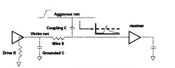
Figure 4 is a typical transmission of erroneous logic of adjacent networks caused by crosstalk pulses. The signal transmitted on the interference source network causes a noise pulse in the interfered network and the receiving end through the coupling capacitor, resulting in an undesirable pulse being sent to the receiving end. If the pulse strength exceeds the trigger value of the receiving end, an uncontrollable trigger pulse will be generated, causing confusion in the logical function of the next level network.
3.2 Timing delay caused by crosstalk
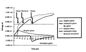
In digital design, timing issues are an important consideration. Figure 5 shows the timing problem caused by crosstalk noise. The lower part of the figure shows two types of noise pulses generated by the interference source network (Helpful Figure 5 Delay glitch caused by crosstalk noise and Unhelpful glitch). When the noise pulse (helpful glitch) is superimposed on the interfered network, it causes the interference network signal transmission delay to decrease; similarly, when the noise pulse (Unhelpful glitch) is superimposed on the interfered network, it increases the delay of the normal transmission signal of the interfered network. Although this crosstalk noise that reduces network transmission delay is helpful for improving PCB timing, in actual PCB design, due to the uncertainty of the interference source network, this delay cannot be controlled, so the delay caused by this crosstalk must be suppressed.
4.Minimize crosstalk
Crosstalk is common in high-speed and high-density PCB design, and the impact of crosstalk on the system is generally negative. To reduce crosstalk, the most basic thing is to make the coupling between the interference source network and the interfered network as small as possible. It is impossible to completely avoid crosstalk in high-density and complex PCB design, but in system design, designers should choose appropriate methods to minimize crosstalk without affecting other system performance. Combined with the above analysis, solving the crosstalk problem mainly considers the following aspects:
(1)Under the condition that the wiring conditions allow, the distance between transmission lines should be increased as much as possible; or the parallel length (accumulated parallel length) between adjacent transmission lines should be reduced as much as possible, preferably between different layers.
(2)The routing directions of the signal layers of two adjacent layers (without plane layer isolation) should be perpendicular, and parallel routing should be avoided as much as possible to reduce crosstalk between layers.
(3)Under the condition of ensuring signal timing, select devices with low conversion speed as much as possible to slow down the rate of change of electric and magnetic fields, thereby reducing crosstalk.
(4)When designing the stacking, under the condition of meeting the characteristic impedance, the dielectric layer between the wiring layer and the reference plane (power or ground plane) should be as thin as possible, thereby increasing the coupling between the transmission line and the reference plane and reducing the coupling between adjacent transmission lines.
(5)Since there is only one reference plane on the surface, the electric field coupling of the surface wiring is stronger than that of the middle layer, so the signal lines that are more sensitive to crosstalk should be laid in the inner layer as much as possible.
(6)By terminating, the impedance of the far-end and near-end terminals of the transmission line can be matched with the transmission line, which can greatly reduce the amplitude of crosstalk.
5.Conclusion
Digital system design has entered a new stage. Many high-speed design issues that were in a secondary position in the past now have a key impact on system performance. Signal integrity issues including crosstalk have brought about changes in design concepts, design processes and design methods. Faced with new challenges, the most critical thing for crosstalk noise is to find out those networks that really affect the normal operation of the system, rather than blindly suppressing crosstalk noise for all networks, which is also inconsistent with limited wiring resources. The crosstalk problem discussed in this article is of great significance for solving crosstalk problems in high-speed and high-density circuit design.


