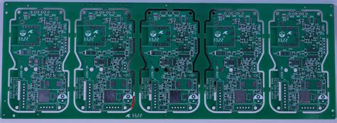
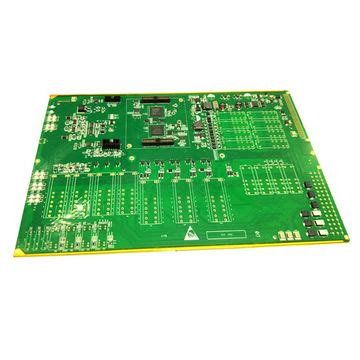
High-speed pcb design
Optimizing Signal Integrity in High-Speed PCB Design

Optimizing signal integrity in high-speed PCB design is a critical aspect that engineers must meticulously address to ensure the reliable performance of electronic systems. As the demand for faster data transmission rates and higher processing speeds continues to escalate, the challenges associated with maintaining signal integrity become increasingly complex. To navigate these challenges, it is essential to understand the fundamental principles and best practices that underpin high-speed PCB design.
One of the primary considerations in high-speed PCB design is the management of signal reflections.
Signal reflections occur when there is a discontinuity in the transmission line, causing a portion of the signal to be reflected back towards the source. This can lead to signal degradation and timing issues, which are detrimental to the overall performance of the system. To mitigate signal reflections, it is crucial to ensure impedance matching throughout the transmission line. This can be achieved by carefully designing the trace width, spacing, and the dielectric properties of the PCB material to match the characteristic impedance of the transmission line.
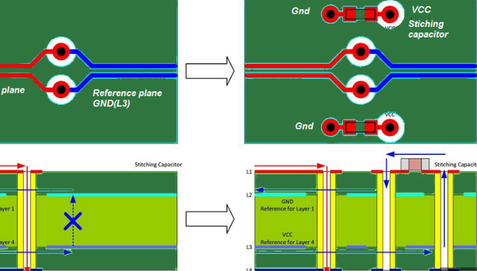
In addition to impedance matching, minimizing crosstalk is another vital aspect of optimizing signal integrity.
Crosstalk refers to the unwanted coupling of signals between adjacent traces, which can result in noise and interference. To reduce crosstalk, designers should maintain adequate spacing between high-speed traces and employ ground planes to provide a return path for the signals. Furthermore, differential signaling can be utilized to enhance noise immunity, as it involves transmitting signals as pairs of complementary signals, thereby canceling out common-mode noise.
Another critical factor in high-speed PCB design is the management of signal attenuation.
Signal attenuation occurs as the signal propagates through the transmission line, leading to a reduction in signal amplitude. This can be exacerbated by factors such as trace length, frequency, and the dielectric properties of the PCB material. To address signal attenuation, designers can use low-loss materials and optimize trace geometry to minimize resistive and dielectric losses. Additionally, the use of signal conditioning techniques, such as pre-emphasis and equalization, can help to compensate for signal degradation over long distances.
Power integrity is also closely related to signal integrity in high-speed PCB design.
Ensuring a stable power supply is essential for maintaining the performance of high-speed circuits. Power distribution networks (PDNs) should be designed to minimize voltage fluctuations and noise. This can be achieved by using decoupling capacitors strategically placed near the power pins of integrated circuits, as well as employing power and ground planes to provide low-impedance paths for current flow. Moreover, careful consideration of the placement and routing of power traces can help to reduce electromagnetic interference (EMI) and improve overall system performance.
Thermal management is another aspect that cannot be overlooked in high-speed PCB design.
As the operating frequencies and power densities increase, effective thermal management becomes crucial to prevent overheating and ensure the longevity of electronic components. Techniques such as the use of thermal vias, heat sinks, and proper airflow management can help to dissipate heat and maintain optimal operating temperatures.
In conclusion, optimizing signal integrity in high-speed PCB design requires a comprehensive understanding of various factors, including impedance matching, crosstalk reduction, signal attenuation management, power integrity, and thermal management. By meticulously addressing these aspects, engineers can design high-speed PCBs that deliver reliable performance and meet the ever-increasing demands of modern electronic systems. Through careful planning, simulation, and adherence to best practices, the challenges associated with high-speed PCB design can be effectively mitigated, ensuring the successful implementation of advanced electronic technologies.
Techniques for Minimizing Crosstalk in High-Speed PCBs
In the realm of high-speed printed circuit board (PCB) design, minimizing crosstalk is a critical concern. Crosstalk, the unwanted coupling of signals between adjacent traces, can lead to signal integrity issues, data corruption, and overall system malfunction. To mitigate these risks, designers employ a variety of techniques that ensure the reliable performance of high-speed PCBs.
One fundamental approach to minimizing crosstalk is to maintain adequate spacing between signal traces.
By increasing the distance between traces, the electromagnetic interference (EMI) that causes crosstalk is significantly reduced. This spacing should be carefully calculated based on the operating frequency and the specific characteristics of the PCB material. Additionally, designers often use ground planes to further isolate signal traces. Ground planes act as a shield, absorbing and dissipating EMI, thereby reducing the potential for crosstalk.
Another effective technique involves the use of differential signaling.
In differential signaling, two complementary signals are transmitted along a pair of traces. The differential pair is designed such that any noise or interference affects both signals equally, allowing the receiver to subtract the noise and recover the original signal. This method not only minimizes crosstalk but also enhances signal integrity, making it particularly useful in high-speed applications.
Moreover, careful routing of signal traces is essential in high-speed PCB design.
Designers should avoid running parallel traces for long distances, as this increases the likelihood of crosstalk. Instead, traces should be routed orthogonally or with sufficient separation. When parallel routing is unavoidable, the use of guard traces can be beneficial. Guard traces are grounded lines placed between signal traces to provide additional shielding and reduce crosstalk.
The choice of PCB materials also plays a significant role in crosstalk mitigation.
High-speed PCBs often utilize low-loss dielectric materials with controlled impedance characteristics. These materials help maintain signal integrity by minimizing signal attenuation and dispersion. Additionally, the use of high-quality vias and connectors ensures that signal paths remain consistent and free from unexpected impedance changes, further reducing the potential for crosstalk.
Furthermore, proper termination of signal traces is crucial in high-speed PCB design.
Impedance mismatches at the ends of traces can cause signal reflections, which contribute to crosstalk. By employing appropriate termination techniques, such as series or parallel termination, designers can match the impedance of the trace to the source and load, thereby minimizing reflections and crosstalk.
In addition to these techniques, the use of simulation and modeling tools is invaluable in high-speed PCB design.
These tools allow designers to predict and analyze crosstalk before the physical board is fabricated. By simulating different routing scenarios and material choices, designers can identify potential crosstalk issues and make informed decisions to mitigate them. This proactive approach not only saves time and resources but also ensures the reliability of the final product.
In conclusion, minimizing crosstalk in high-speed PCBs requires a multifaceted approach that encompasses trace spacing, differential signaling, careful routing, material selection, proper termination, and the use of simulation tools. By employing these techniques, designers can effectively reduce crosstalk, ensuring the integrity and performance of high-speed electronic systems. As technology continues to advance, the importance of these techniques will only grow, making them essential knowledge for any PCB designer working in the high-speed domain.
Best Practices for Power Distribution in High-Speed PCB Layouts
In the realm of high-speed PCB design, effective power distribution is paramount to ensuring optimal performance and reliability. As electronic devices continue to evolve, the demand for faster processing speeds and higher data rates necessitates meticulous attention to power distribution strategies. To achieve this, several best practices must be adhered to, each contributing to the overall integrity and functionality of the PCB.
Firstly, it is essential to recognize the importance of a well-designed power distribution network (PDN).
A robust PDN minimizes voltage drops and noise, which are critical factors in high-speed circuits. One fundamental practice is to use multiple power and ground planes. These planes provide low impedance paths for current flow, thereby reducing the potential for voltage fluctuations. Additionally, they offer excellent shielding against electromagnetic interference (EMI), which is particularly beneficial in high-speed environments.
Transitioning to the layout phase, careful placement of decoupling capacitors is crucial.
These capacitors serve to filter out noise and provide a stable voltage supply to the integrated circuits (ICs). It is advisable to place decoupling capacitors as close as possible to the power pins of the ICs. This proximity minimizes the inductance of the connection, enhancing the capacitor’s effectiveness. Furthermore, using a range of capacitor values can help address different frequency components of the noise, ensuring comprehensive filtering.
Another best practice involves the use of power islands or power polygons.
These are dedicated areas on the PCB that distribute power to specific sections of the circuit. By isolating different power domains, power islands help to prevent noise from propagating across the entire board. This isolation is particularly beneficial in mixed-signal designs, where analog and digital circuits coexist. Power islands can be connected to the main power plane through vias, which should be strategically placed to optimize current flow and minimize impedance.
In addition to these layout considerations, attention must be given to the selection of power components.
Voltage regulators, for instance, should be chosen based on their ability to provide a stable output with minimal ripple. Low-dropout (LDO) regulators are often preferred in high-speed designs due to their low noise characteristics. However, switching regulators may be necessary for higher efficiency, especially in power-hungry applications. In such cases, careful filtering and shielding are required to mitigate the noise generated by the switching process.
Thermal management is another critical aspect of power distribution in high-speed PCB layouts.
High-speed circuits tend to generate significant heat, which can adversely affect performance and reliability. To address this, designers should incorporate thermal vias and heat sinks to dissipate heat effectively. Additionally, spreading power components across the PCB can help distribute heat more evenly, preventing hotspots that could lead to thermal stress and potential failure.
Lastly, simulation and analysis tools play a vital role in optimizing power distribution.
Tools such as power integrity (PI) simulators allow designers to model the PDN and identify potential issues before fabrication. These simulations can reveal areas of high impedance, excessive noise, or thermal hotspots, enabling designers to make informed adjustments to the layout. By leveraging these tools, designers can ensure that the final PCB meets the stringent requirements of high-speed applications.
In conclusion, effective power distribution in high-speed PCB layouts is a multifaceted challenge that requires careful planning and execution. By adhering to best practices such as using multiple power and ground planes, strategically placing decoupling capacitors, employing power islands, selecting appropriate power components, managing thermal effects, and utilizing simulation tools, designers can create robust and reliable high-speed PCBs. These practices not only enhance performance but also contribute to the longevity and dependability of the electronic devices they power.
Importance of Controlled Impedance in High-Speed PCB Design
In the realm of high-speed PCB design, the importance of controlled impedance cannot be overstated. As electronic devices continue to evolve, the demand for faster data transmission rates and higher signal integrity has become paramount. Controlled impedance is a critical factor in ensuring that high-speed signals are transmitted with minimal distortion and loss, thereby maintaining the integrity of the data being communicated.
To understand the significance of controlled impedance, it is essential to first grasp the concept of impedance itself.
Impedance is the measure of opposition that a circuit presents to the flow of alternating current (AC) and is a combination of resistance, inductance, and capacitance. In high-speed PCB design, the impedance of a transmission line must be carefully controlled to match the impedance of the source and load. This matching is crucial because any mismatch can result in signal reflections, which can degrade the signal quality and lead to data errors.
One of the primary reasons controlled impedance is vital in high-speed PCB design is the need to minimize signal reflections.
When a signal travels along a transmission line with a consistent impedance, it reaches the load without significant reflections. However, if there is an impedance mismatch, part of the signal is reflected back towards the source, causing interference and potential data corruption. By maintaining controlled impedance, designers can ensure that the signal reaches its destination with minimal distortion, thereby preserving the integrity of the data.
Moreover, controlled impedance plays a significant role in reducing electromagnetic interference (EMI).
High-speed signals can generate electromagnetic fields that may interfere with other components on the PCB or with external devices. By carefully controlling the impedance of the transmission lines, designers can minimize the generation of these electromagnetic fields, thereby reducing the potential for EMI. This is particularly important in applications where signal integrity and reliability are critical, such as in telecommunications, aerospace, and medical devices.
In addition to minimizing signal reflections and reducing EMI, controlled impedance is also essential for maintaining signal integrity over long distances.
As the frequency of the signal increases, the effects of the transmission line’s impedance become more pronounced. High-speed signals are more susceptible to attenuation and distortion, which can degrade the quality of the transmitted data. By ensuring that the impedance of the transmission line is consistent, designers can mitigate these effects and maintain the integrity of the signal over longer distances.
Furthermore, controlled impedance is crucial for achieving consistent performance across different manufacturing batches.
Variations in the PCB manufacturing process can lead to differences in the impedance of the transmission lines, which can affect the performance of the final product. By specifying controlled impedance requirements, designers can ensure that the PCB manufacturer adheres to strict guidelines, resulting in consistent and reliable performance across different production runs.
In conclusion, the importance of controlled impedance in high-speed PCB design cannot be underestimated. It is a critical factor in minimizing signal reflections, reducing electromagnetic interference, maintaining signal integrity over long distances, and ensuring consistent performance across different manufacturing batches. As electronic devices continue to demand higher data transmission rates and greater signal integrity, the need for controlled impedance in high-speed PCB design will only become more pronounced. By understanding and implementing controlled impedance principles, designers can create PCBs that meet the rigorous demands of modern high-speed electronic applications.