High-speed PCB design
(I) Challenges faced by electronic system design
With the large-scale increase in system design complexity and integration, electronic system designers are engaged in circuit design above 100MHZ, and the operating frequency of the bus has reached or exceeded 50MHZ, and some even exceed 100MHZ. Currently, about 50% of the designs have a clock frequency exceeding 50MHz, and nearly 20% of the designs have a main frequency exceeding 120MHz.
When the system operates at 50MHz, transmission line effects and signal integrity problems will occur; and when the system clock reaches 120MHz, unless high-speed circuit design knowledge is used, the PCB designed based on traditional methods will not work. Therefore, high-speed circuit design technology has become a design method that electronic system designers must adopt. Only by using the design technology of high-speed circuit designers can the controllability of the design process be achieved.

(II) What is a high-speed circuit?
It is generally believed that if the frequency of a digital logic circuit reaches or exceeds 45MHZ”50MHZ, and the circuit operating at this frequency accounts for a certain proportion of the entire electronic system (for example, 1/3), it is called a high-speed circuit.
In fact, the harmonic frequency of the signal edge is higher than the frequency of the signal itself. It is the rising and falling edges of the signal that change rapidly (or the signal jump) that trigger the unexpected results of signal transmission. Therefore, it is usually agreed that if the line propagation delay is greater than 1/2 of the rise time of the digital signal driver, such a signal is considered to be a high-speed signal and produces a transmission line effect. .
Signal transmission occurs at the moment when the signal state changes, such as the rise or fall time. The signal travels from the driver to the receiver for a fixed period of time. If the transmission time is less than 1/2 of the rise or fall time, the reflected signal from the receiver will reach the driver before the signal changes state. Conversely, the reflected signal will reach the driver after the signal changes state. If the reflected signal is strong, the superimposed waveform may change the logic state.
(III) Determination of high-speed signals
Above, we defined the prerequisites for the occurrence of the transmission line effect, but how do we know whether the line delay is greater than 1/2 of the signal rise time at the driver? Generally, the typical value of the signal rise time can be given in the device manual, while the signal propagation time is determined by the actual wiring length in PCB design. The following figure shows the correspondence between the signal rise time and the allowable wiring length (delay).
The delay per unit inch on the PCB board is 0.167ns. However, if there are many vias, many device pins, and many constraints set on the network line, the delay will increase. Usually the signal rise time of high-speed logic devices is about 0.2ns. If there is a GaAs chip on the board, the maximum wiring length is 7.62mm.
Let Tr be the signal rise time, Tpd = is the propagation delay of the signal line. If Tr≥4Tpd, the signal falls in the safe area. If 2Tpd≥Tr≥4Tpd, the signal falls in the uncertain area. If Tr≤2Tpd, the signal falls in the problem area. For signals falling in the uncertain area and the problem area, high-speed wiring methods should be used.
(IV) What is a transmission line
The routing on the PCB board can be equivalent to the series and parallel capacitor, resistor and inductor structure shown in the figure below. The typical value of the series resistor is 0.25-0.55 ohms/foot, because of the insulation layer, the parallel resistance is usually very high. After adding parasitic resistance, capacitance and inductance to the actual PCB connection, the final impedance on the connection is called characteristic impedance Zo. The wider the wire diameter, the closer to the power supply/ground, or the higher the dielectric constant of the isolation layer, the smaller the characteristic impedance. If the impedance of the transmission line and the receiving end do not match, the output current signal and the final stable state of the signal will be different, which will cause the signal to be reflected at the receiving end. This reflected signal will be transmitted back to the signal transmitting end and reflected back again. As the energy decreases, the amplitude of the reflected signal will decrease until the voltage and current of the signal reach stability. This effect is called oscillation, and the oscillation of the signal can often be seen on the rising and falling edges of the signal.
(V) Transmission line effect
Based on the transmission line model defined above, in summary, the transmission line will have the following effects on the entire circuit design.
· Reflected signals
· Delay & Timing errors
· False Switching
· Overshoot/Undershoot
· Induced Noise (or crosstalk)
· EMI radiation
5.1 Reflected signals
If a trace is not terminated correctly (terminal matching), the signal pulse from the driver end is reflected at the receiving end, causing unexpected effects and distorting the signal profile. When the distortion is very significant, it can cause a variety of errors and cause design failure. At the same time, the sensitivity of the distorted signal to noise increases, which can also cause design failure. If the above situation is not considered enough, EMI will increase significantly, which will not only affect the design results itself, but also cause the failure of the entire system.
The main reasons for the generation of reflected signals: too long traces; transmission lines that are not matched and terminated, excessive capacitance or inductance, and impedance mismatch.
5.2 Delay and Timing Errors
Signal delay and timing errors are manifested as: the signal does not jump for a period of time when it changes between the high and low thresholds of the logic level. Excessive signal delay may cause timing errors and confusion of device functions.
Problems usually occur when there are multiple receiving ends. Circuit designers must determine the worst-case time delay to ensure the correctness of the design. Causes of signal delay: driver overload, long routing.
5.3 Multiple crossing logic level threshold errors
The signal may cross the logic level threshold multiple times during the transition process, resulting in this type of error. Multiple crossing logic level threshold errors are a special form of signal oscillation, that is, the oscillation of the signal occurs near the logic level threshold, and multiple crossings of the logic level threshold will cause logic function disorder. Causes of reflected signals: too long routing, unterminated transmission lines, excessive capacitance or inductance, and impedance mismatch.
5.4 Overshoot and undershoot
Overshoot and undershoot come from two reasons: too long routing or too fast signal changes. Although most components have input protection diodes at the receiving end, sometimes these overshoot levels will far exceed the component power supply voltage range and damage the components.
5.5 Crosstalk
Crosstalk is manifested as a signal passing through a signal line, and a related signal will be induced on the adjacent signal line on the PCB board, which we call crosstalk.
The closer the signal line is to the ground line and the larger the line spacing, the smaller the crosstalk signal generated. Asynchronous signals and clock signals are more likely to generate crosstalk. Therefore, the way to resolve crosstalk is to remove the signal that causes crosstalk or shield the signal that is severely interfered.
5.6 Electromagnetic Radiation
EMI (Electro-Magnetic Interference) is electromagnetic interference, and the problems it causes include excessive electromagnetic radiation and sensitivity to electromagnetic radiation. EMI is manifested as the radiation of electromagnetic waves to the surrounding environment when the digital system is powered on, thereby interfering with the normal operation of electronic equipment in the surrounding environment. The main reason for its occurrence is that the circuit operating frequency is too high and the layout and wiring are unreasonable. At present, there are software tools for EMI simulation, but EMI simulators are very expensive, and it is difficult to set simulation parameters and boundary conditions, which will directly affect the accuracy and practicality of the simulation results. The most common practice is to apply various design rules for controlling EMI to every link of the design, so as to achieve rule-driven and control in every link of the design.
(VI) Methods to avoid transmission line effects
In view of the influences introduced by the above transmission line problems, we will discuss the methods to control these influences from the following aspects.
6.1 Strictly control the routing length of key network cables
If there are high-speed jump edges in the design, it is necessary to consider the problem of transmission line effects on the PCB board. The fast integrated circuit chips with very high clock frequencies that are commonly used now have such problems. There are some basic principles to solve this problem: If CMOS or TTL circuits are used for design, the wiring length should not exceed 7 inches. The wiring length should not exceed 1.5 inches when the operating frequency is 50MHz. If the operating frequency reaches or exceeds 75MHz, the wiring length should be 1 inch. For GaAs chips, the maximum wiring length should be 0.3 inches. If this standard is exceeded, there is a transmission line problem.
6.2 Reasonable planning of routing topology
Another way to solve the transmission line effect is to choose the correct wiring path and terminal topology. The topology of the routing refers to the routing sequence and routing structure of a network cable. When using high-speed logic devices, unless the routing branch length is kept very short, the signal with fast edge changes will be distorted by the branch routing on the signal trunk routing. Under normal circumstances, PCB routing adopts two basic topologies, namely daisy chain routing and star distribution.
For daisy chain routing, the routing starts from the driver end and reaches each receiving end in turn. If a series resistor is used to change the signal characteristics, the position of the series resistor should be close to the driver end. Daisy chain routing is the best in controlling the high-order harmonic interference of the routing. However, this routing method has the lowest routing rate and is not easy to be 100% routed. In actual design, we make the branch length in daisy chain routing as short as possible, and the safe length value should be: Stub Delay <= Trt *0.1.
For example, the branch end length in a high-speed TTL circuit should be less than 1.5 inches. This topology occupies less wiring space and can be terminated with a single resistor matching. However, this routing structure makes the reception of signals at different signal receiving ends asynchronous.
Star topology can effectively avoid the problem of asynchronous clock signals, but it is very difficult to complete the wiring manually on a high-density PCB board. Using an automatic router is the best way to complete star wiring. Terminal resistance is required on each branch. The resistance of the terminal resistance should match the characteristic impedance of the connection. This can be calculated manually or by using CAD tools to calculate the characteristic impedance value and the terminal matching resistance value.
Simple terminal resistance is used in the above two examples.
In practice, more complex matching terminals can be used. The first option is RC matching terminal. RC matching terminal can reduce power consumption, but can only be used in cases where the signal is relatively stable. This method is most suitable for matching clock line signals. The disadvantage is that the capacitance in the RC matching terminal may affect the shape and propagation speed of the signal.
Series resistance matching terminal does not generate additional power consumption, but it slows down the transmission of the signal. This method is used in bus driving circuits where time delay has little effect. The advantage of series resistance matching terminal is that it can reduce the number of components used on the board and the connection density.
The last method is to separate the matching terminal.
In this method, the matching component needs to be placed near the receiving end. Its advantage is that it will not pull down the signal and can avoid noise well. It is typically used for TTL input signals (ACT, HCT, FAST).
In addition, the package type and mounting type of the terminal matching resistor must also be considered. Generally, SMD surface mount resistors have lower inductance than through-hole components, so SMD package components are the first choice. If you choose ordinary plug-in resistors, there are also two mounting methods to choose from: vertical and horizontal.
In the vertical mounting method, one of the mounting pins of the resistor is very short, which can reduce the thermal resistance between the resistor and the circuit board, making it easier for the heat of the resistor to dissipate into the air. However, the longer vertical mounting will increase the inductance of the resistor. The horizontal mounting method has lower inductance due to the lower mounting. However, overheated resistors will drift, and in the worst case, the resistor will become an open circuit, causing the PCB trace termination matching to fail, becoming a potential failure factor.
6.3 Methods to suppress electromagnetic interference
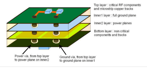
Solving the signal integrity problem well will improve the electromagnetic compatibility (EMC) of the PCB board. It is very important to ensure that the PCB board has good grounding. For complex designs, it is very effective to use a signal layer with a ground layer. In addition, minimizing the density of the outermost signal of the circuit board is also a good way to reduce electromagnetic radiation. This method can be achieved by using the “surface layering” technology “Build-up” design to make PCBs. Surface layering is achieved by adding a thin insulating layer and a combination of micro-holes used to penetrate these layers on the ordinary process PCB. The resistors and capacitors can be buried under the surface layer, and the trace density per unit area will increase by nearly one-fold, thereby reducing the volume of the PCB.
The reduction of PCB area has a huge impact on the topology of the trace, which means a smaller current loop, a smaller branch trace length, and electromagnetic radiation is approximately proportional to the area of the current loop; at the same time, the small volume feature means that high-density pin packaging devices can be used, which in turn reduces the connection length, thereby reducing the current loop and improving the electromagnetic compatibility characteristics.

6.4 Other technologies that can be used
In order to reduce the instantaneous overshoot of the voltage on the power supply of the integrated circuit chip, a decoupling capacitor should be added to the integrated circuit chip. This can effectively remove the impact of the burrs on the power supply and reduce the radiation of the power supply loop on the printed circuit board.
When the decoupling capacitor is directly connected to the power leg of the integrated circuit instead of the power layer, its burr smoothing effect is best. This is why some device sockets have decoupling capacitors, while some devices require the decoupling capacitor to be close enough to the device.
Any high-speed and high-power devices should be placed together as much as possible to reduce the instantaneous overshoot of the power supply voltage.
If there is no power layer, the long power connection will form a loop between the signal and the return line, becoming a radiation source and an easily inductive circuit.
The situation where the routing forms a loop that does not pass through the same network cable or other routings is called an open loop. If the loop passes through other routings of the same network cable, it forms a closed loop. Both situations will form an antenna effect (wire antenna and loop antenna). The antenna generates EMI radiation to the outside and is also a sensitive circuit itself. The closed loop is an issue that must be considered because the radiation it generates is approximately proportional to the closed loop area.
Conclusion
High-speed circuit design is a very complex design process. ZUKEN’s high-speed circuit routing algorithm (Route Editor) and EMC/EMI analysis software (INCASES, Hot-Stage) are used to analyze and find problems. The method described in this article is specifically designed to solve these high-speed circuit design problems. In addition, there are multiple factors that need to be considered when designing high-speed circuits, and these factors are sometimes contradictory. For example, if high-speed devices are placed close together during layout, although delays can be reduced, crosstalk and significant thermal effects may occur. Therefore, in the design, it is necessary to weigh various factors and make a comprehensive compromise; both to meet the design requirements and to reduce the design complexity. The use of high-speed PCB design methods constitutes the controllability of the design process. Only controllable ones can be Only if you are reliable can you be successful!