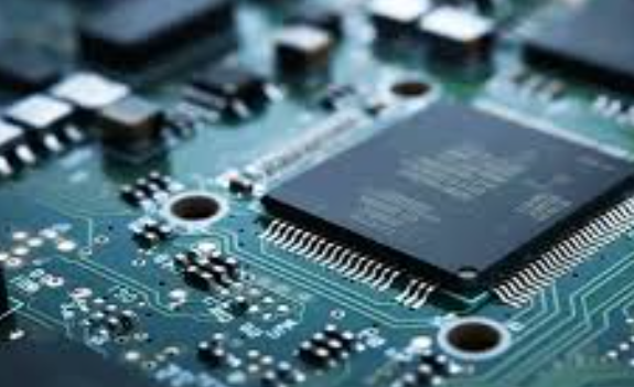
High-speed pcb design guide
Understanding Signal Integrity in High-Speed PCB Design
In the realm of high-speed PCB design, understanding signal integrity is paramount to ensuring the optimal performance of electronic circuits. Signal integrity refers to the quality and reliability of electrical signals as they traverse through the PCB, and it becomes increasingly critical as the speed of the signals increases. High-speed signals are susceptible to various forms of degradation, including reflections, crosstalk, and electromagnetic interference (EMI), which can significantly impact the functionality of the circuit.
To begin with, reflections occur when a signal encounters an impedance mismatch along its transmission path.
This mismatch can cause a portion of the signal to be reflected back towards the source, leading to signal distortion and potential data errors. To mitigate reflections, it is essential to maintain consistent impedance throughout the signal path. This can be achieved by carefully designing the trace widths and spacing, as well as by using controlled impedance techniques. Additionally, proper termination of signal lines, either through series or parallel termination methods, can help absorb reflected signals and preserve signal integrity.
Crosstalk, another critical factor in high-speed PCB design, arises when a signal on one trace induces an unwanted signal on an adjacent trace.
This phenomenon is particularly problematic in densely packed PCBs where traces are in close proximity. To minimize crosstalk, designers should consider increasing the spacing between high-speed traces and employing differential signaling, which uses pairs of traces to carry signals in opposite phases. Differential signaling not only reduces crosstalk but also enhances noise immunity, making it a preferred choice for high-speed applications.
Electromagnetic interference (EMI) is yet another challenge that can compromise signal integrity.
EMI is the result of electromagnetic radiation emitted by high-speed signals, which can interfere with other electronic components and systems. To combat EMI, designers should implement proper grounding and shielding techniques. A solid ground plane can provide a low-impedance return path for signals, reducing the potential for EMI. Additionally, placing ground vias strategically around high-speed traces and using ground fills can further enhance EMI suppression.
Transitioning to the layout considerations, the placement of components plays a crucial role in maintaining signal integrity.
High-speed components should be positioned as close to each other as possible to minimize the length of high-speed traces, thereby reducing the potential for signal degradation. Furthermore, critical signal paths should be kept short and direct, avoiding unnecessary bends and vias that can introduce impedance discontinuities.
The choice of materials also influences signal integrity in high-speed PCB design.
High-frequency signals are more sensitive to the dielectric properties of the PCB substrate. Therefore, selecting materials with low dielectric constant (Dk) and low dissipation factor (Df) can help maintain signal integrity by reducing signal loss and dispersion. Additionally, using high-quality copper with smooth surface finishes can minimize signal attenuation and improve overall performance.
Simulation and modeling tools are indispensable in the design process, allowing engineers to predict and analyze signal integrity issues before physical prototyping.
Tools such as signal integrity simulators and electromagnetic field solvers can provide valuable insights into the behavior of high-speed signals, enabling designers to make informed decisions and optimize their PCB layouts accordingly.
In conclusion, understanding and addressing signal integrity is essential for successful high-speed PCB design. By carefully managing impedance, minimizing crosstalk, mitigating EMI, optimizing component placement, selecting appropriate materials, and leveraging simulation tools, designers can ensure that their high-speed circuits perform reliably and efficiently. As technology continues to advance, the importance of signal integrity in high-speed PCB design will only grow, making it a critical area of focus for engineers and designers alike.
Best Practices for Layer Stackup in High-Speed PCB Design
In high-speed PCB design, the layer stackup plays a crucial role in ensuring signal integrity, minimizing electromagnetic interference (EMI), and achieving optimal performance. A well-thought-out layer stackup can significantly enhance the electrical characteristics of the PCB, thereby improving the overall functionality of the electronic device. To begin with, it is essential to understand that the layer stackup refers to the arrangement of conductive and insulating layers within a PCB. This arrangement determines the path of signal transmission and the distribution of power and ground planes, which are critical for high-speed applications.
One of the best practices in layer stackup design is to maintain symmetry.
Symmetrical stackups help in reducing warpage during the manufacturing process, which is particularly important for high-speed PCBs where even slight deformations can lead to signal integrity issues. Additionally, symmetry ensures that the mechanical properties of the PCB are balanced, thereby enhancing its reliability and durability.
Another key consideration is the placement of power and ground planes.
It is advisable to place these planes adjacent to each other, separated by a thin dielectric layer. This configuration creates a low-inductance path for the return currents, which is essential for maintaining signal integrity at high frequencies. Moreover, closely spaced power and ground planes form a high-frequency decoupling capacitor, which helps in reducing noise and EMI.
Transitioning to the topic of signal layers, it is important to route high-speed signals on inner layers sandwiched between ground planes.
This technique, known as stripline routing, provides better shielding against external noise and reduces crosstalk between adjacent signal traces. In contrast, microstrip routing, where signals are routed on outer layers, is more susceptible to EMI and should be used cautiously in high-speed designs.
Furthermore, the dielectric material used in the PCB stackup significantly impacts signal integrity.
Materials with low dielectric constant (Dk) and low dissipation factor (Df) are preferred for high-speed applications as they offer lower signal loss and better impedance control. It is also crucial to ensure that the dielectric thickness is consistent across the PCB to maintain uniform impedance, which is vital for high-speed signal transmission.
In addition to material selection, the aspect of impedance control cannot be overlooked.
Controlled impedance is necessary to match the impedance of the transmission lines with that of the source and load, thereby minimizing signal reflections and ensuring signal integrity. This can be achieved by carefully designing the trace width, spacing, and the dielectric thickness between the signal layers and the reference planes.
Moreover, it is beneficial to incorporate multiple ground planes in the layer stackup.
Multiple ground planes provide additional paths for return currents, thereby reducing the loop area and minimizing EMI. They also enhance the thermal performance of the PCB by providing better heat dissipation.
Lastly, it is important to consider the manufacturability of the PCB when designing the layer stackup.
Complex stackups with numerous layers and tight tolerances can be challenging to manufacture and may result in higher costs and longer lead times. Therefore, it is advisable to collaborate with PCB manufacturers early in the design process to ensure that the stackup is both electrically optimal and manufacturable.
In conclusion, a well-designed layer stackup is fundamental to the success of high-speed PCB designs. By adhering to best practices such as maintaining symmetry, optimizing the placement of power and ground planes, using appropriate dielectric materials, ensuring controlled impedance, and considering manufacturability, designers can achieve superior signal integrity, reduced EMI, and enhanced overall performance of their high-speed PCBs.

Techniques for Minimizing Crosstalk in High-Speed PCB Layouts
In the realm of high-speed PCB design, minimizing crosstalk is paramount to ensuring signal integrity and overall system performance. Crosstalk, the unwanted coupling of signals between adjacent traces, can lead to data corruption, timing errors, and electromagnetic interference. To mitigate these issues, designers must employ a variety of techniques that address the root causes of crosstalk and enhance the robustness of the PCB layout.
One fundamental technique for minimizing crosstalk is to maintain adequate spacing between signal traces.
By increasing the distance between adjacent traces, the capacitive and inductive coupling that causes crosstalk is significantly reduced. This approach is particularly effective in high-speed designs where signal integrity is critical. Additionally, designers should consider the use of differential pairs for high-speed signals. Differential signaling inherently reduces crosstalk because the signals are transmitted in pairs with opposite polarities, which cancels out the noise induced by adjacent traces.
Another crucial method involves the strategic placement of ground planes.
Ground planes act as a shield, absorbing and dissipating the electromagnetic interference that contributes to crosstalk. Ensuring that signal traces are routed over a continuous ground plane can greatly reduce the coupling between them. Moreover, the use of multiple ground planes in a multilayer PCB design can further enhance this shielding effect. It is also advisable to place ground vias near critical signal traces to provide a low-impedance return path, thereby minimizing the loop area and reducing the potential for crosstalk.
In addition to spacing and grounding techniques, careful consideration of trace routing is essential.
Designers should avoid running high-speed signal traces in parallel for extended distances, as this increases the likelihood of crosstalk. Instead, traces should be routed orthogonally on adjacent layers to minimize coupling. When parallel routing is unavoidable, incorporating guard traces—grounded traces placed between signal lines—can serve as an effective barrier to crosstalk. These guard traces absorb and redirect the electromagnetic interference, thereby protecting the integrity of the signal traces.
The use of controlled impedance traces is another effective strategy.
By designing traces with a specific impedance, matched to the source and load, signal reflections and the associated crosstalk can be minimized. This requires precise control over trace width, spacing, and the dielectric properties of the PCB material. Tools such as impedance calculators and simulation software can aid designers in achieving the desired impedance characteristics.
Furthermore, the implementation of proper termination techniques can play a significant role in reducing crosstalk.
Termination resistors, placed at the end of signal lines, help to match the impedance and prevent signal reflections that contribute to crosstalk. Series termination, parallel termination, and Thevenin termination are common methods that can be employed based on the specific requirements of the design.
Lastly, signal integrity analysis and simulation are indispensable tools in the high-speed PCB design process.
By simulating the PCB layout, designers can identify potential crosstalk issues and make necessary adjustments before fabrication. This proactive approach allows for the optimization of trace routing, spacing, and termination, ensuring that the final design meets the stringent requirements of high-speed applications.
In conclusion, minimizing crosstalk in high-speed PCB layouts requires a multifaceted approach that includes adequate trace spacing, strategic use of ground planes, careful trace routing, controlled impedance design, proper termination techniques, and thorough signal integrity analysis. By employing these techniques, designers can significantly enhance the performance and reliability of high-speed PCBs, ensuring that they meet the demands of modern electronic systems.
Effective Power Distribution Strategies in High-Speed PCB Design
Effective power distribution is a critical aspect of high-speed PCB design, as it directly influences the performance, reliability, and electromagnetic compatibility (EMC) of the final product. To achieve optimal power distribution, designers must consider several key strategies that ensure stable and efficient power delivery to all components on the board.
One fundamental approach is the implementation of a well-designed power distribution network (PDN).
A robust PDN minimizes voltage drops and noise, providing a stable power supply to high-speed circuits. This can be achieved by using multiple power and ground planes, which reduce impedance and enhance current-carrying capacity. Additionally, the use of decoupling capacitors is essential in mitigating high-frequency noise and maintaining voltage stability. These capacitors should be strategically placed close to the power pins of integrated circuits (ICs) to be most effective.
Another important strategy involves the careful routing of power and ground traces.
Ensuring that these traces are wide enough to handle the required current without significant voltage drops is crucial. Moreover, maintaining a low-inductance path by minimizing the loop area between power and ground traces helps in reducing electromagnetic interference (EMI). It is also advisable to use a star grounding scheme, where all ground connections converge at a single point, to prevent ground loops and potential noise issues.
Thermal management is another critical consideration in high-speed PCB design.
Efficient power distribution must account for the heat generated by high-speed components. Utilizing thermal vias and heat sinks can help dissipate heat effectively, preventing thermal-related performance degradation. Additionally, selecting materials with high thermal conductivity for the PCB substrate can further enhance heat dissipation.
Signal integrity is closely linked to power distribution, as poor power delivery can lead to signal degradation and timing issues.
To maintain signal integrity, it is important to ensure that the power supply is free from noise and transients. This can be achieved by using low-ESR (Equivalent Series Resistance) capacitors and ferrite beads to filter out high-frequency noise. Furthermore, maintaining a consistent impedance throughout the power distribution network helps in reducing reflections and signal loss.
Incorporating power integrity analysis during the design phase is also crucial.
Simulation tools can be used to model the PDN and identify potential issues such as voltage drops, noise, and resonances. By addressing these issues early in the design process, designers can avoid costly revisions and ensure a reliable final product.
Moreover, collaboration between different design teams, such as PCB layout, signal integrity, and power integrity teams, is essential for effective power distribution. This collaborative approach ensures that all aspects of the design are considered, and potential issues are addressed comprehensively.
In conclusion, effective power distribution in high-speed PCB design requires a multifaceted approach that includes a well-designed PDN, careful routing of power and ground traces, efficient thermal management, and maintaining signal integrity. By implementing these strategies and utilizing simulation tools, designers can achieve stable and efficient power delivery, ensuring the performance and reliability of high-speed electronic devices.


