High-Speed PCB Design: Principles, Challenges, and Best Practices
Introduction
Printed Circuit Boards (PCBs) are the backbone of modern electronics, enabling the interconnection of components and the transmission of signals across devices. As technology advances, the demand for faster and more efficient electronic systems has led to the development of high-speed PCBs. These PCBs are designed to handle signals with high frequencies, often in the range of gigahertz (GHz), and are critical in applications such as telecommunications, computing, automotive systems, and consumer electronics.
High-speed PCB design is a specialized field that requires a deep understanding of signal integrity, power integrity, electromagnetic compatibility (EMC), and thermal management. This article explores the principles, challenges, and best practices associated with high-speed PCB design, providing insights for engineers and designers working in this complex and rapidly evolving domain.
1. Understanding High-Speed PCB Design
High-speed PCB design refers to the process of creating circuit boards that can reliably transmit high-frequency signals without significant degradation. The term “high-speed” is relative and depends on the application, but it generally refers to signals with frequencies above 50 MHz. At these frequencies, the behavior of signals on the PCB becomes more complex, and traditional design rules may no longer apply.
1.1 Signal Integrity
Signal integrity (SI) is a critical aspect of high-speed PCB design. It refers to the quality of the electrical signals as they travel through the PCB. At high frequencies, signals are more susceptible to issues such as reflections, crosstalk, and attenuation, which can degrade performance and lead to errors in data transmission.
1.2 Power Integrity
Power integrity (PI) is another key consideration in high-speed PCB design. It involves ensuring that the power distribution network (PDN) delivers stable and clean power to all components on the board. Poor power integrity can lead to voltage fluctuations, noise, and ultimately, system failures.
1.3 Electromagnetic Compatibility
Electromagnetic compatibility (EMC) is the ability of the PCB to function correctly in its electromagnetic environment without causing or suffering from electromagnetic interference (EMI). High-speed PCBs are particularly prone to EMI due to the high-frequency signals they carry, making EMC a critical design consideration.
1.4 Thermal Management
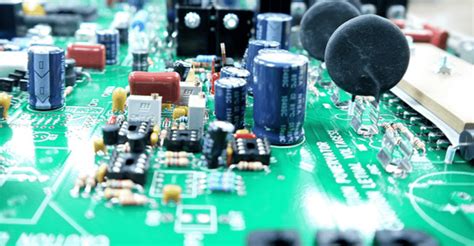
High-speed PCBs often generate significant heat due to the high power consumption of components and the rapid switching of signals. Effective thermal management is essential to prevent overheating, which can lead to component failure and reduced reliability.

2. Challenges in High-Speed PCB Design
Designing high-speed PCBs presents several challenges that require careful consideration and advanced techniques to overcome.
2.1 Signal Reflections and Impedance Matching
Signal reflections occur when there is a mismatch in impedance between the transmission line and the load. This can cause signal distortion and degrade performance. Impedance matching is crucial to minimize reflections and ensure signal integrity. Techniques such as controlled impedance routing and the use of termination resistors are commonly employed to address this issue.
2.2 Crosstalk
Crosstalk is the unwanted coupling of signals between adjacent traces on the PCB. It can lead to signal interference and data errors. To mitigate crosstalk, designers must carefully plan the layout of traces, maintain adequate spacing between them, and use ground planes to shield sensitive signals.
2.3 Power Distribution Network Design
Designing an effective power distribution network is challenging in high-speed PCBs due to the need to deliver stable power to high-speed components. The PDN must have low impedance across a wide frequency range to prevent voltage drops and noise. This requires careful selection of decoupling capacitors, power planes, and vias.
2.4 EMI and EMC Compliance
High-speed PCBs are prone to EMI, which can interfere with other electronic devices and lead to compliance issues. Designers must take steps to minimize EMI, such as using proper grounding techniques, shielding sensitive components, and following EMC design guidelines.
2.5 Thermal Management
Managing heat in high-speed PCBs is critical to ensure reliable operation. High-speed components, such as processors and FPGAs, generate significant heat, and the PCB must be designed to dissipate this heat effectively. Techniques such as thermal vias, heat sinks, and proper component placement are essential for effective thermal management.
3. Best Practices in High-Speed PCB Design
To address the challenges of high-speed PCB design, engineers and designers must follow best practices that ensure signal integrity, power integrity, EMC compliance, and thermal management.
3.1 Controlled Impedance Routing
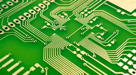
Controlled impedance routing is essential for maintaining signal integrity in high-speed PCBs. This involves designing transmission lines with specific impedance values that match the source and load impedances. The impedance of a transmission line depends on factors such as trace width, dielectric constant, and the distance to the reference plane. Designers must carefully calculate and control these parameters to achieve the desired impedance.
3.2 Proper Layer Stackup
The layer stackup of a PCB plays a crucial role in high-speed design. A well-designed stackup can help minimize crosstalk, reduce EMI, and improve signal integrity. Typically, high-speed PCBs use multiple layers, with dedicated signal, power, and ground planes. The arrangement of these layers should be optimized to provide a low-impedance return path for high-speed signals and to minimize electromagnetic interference.
3.3 Decoupling and Bypass Capacitors
Decoupling and bypass capacitors are essential for maintaining power integrity in high-speed PCBs. These capacitors are placed close to high-speed components to provide a local source of charge and to filter out high-frequency noise. The selection and placement of decoupling capacitors must be carefully considered to ensure effective power delivery and noise suppression.
3.4 Grounding and Shielding
Proper grounding and shielding are critical for minimizing EMI and ensuring EMC compliance. High-speed PCBs should have a solid ground plane that provides a low-impedance return path for signals. Additionally, sensitive signals should be shielded using ground planes or guard traces to prevent crosstalk and EMI.
3.5 Signal Integrity Analysis
Signal integrity analysis is a crucial step in high-speed PCB design. This involves simulating the behavior of signals on the PCB to identify potential issues such as reflections, crosstalk, and timing violations. Tools such as SPICE simulations, time-domain reflectometry (TDR), and eye diagram analysis can be used to evaluate signal integrity and optimize the design.
3.6 Thermal Management Techniques
Effective thermal management is essential for high-speed PCBs to prevent overheating and ensure reliable operation. Designers should consider the thermal properties of the PCB materials, the placement of heat-generating components, and the use of thermal vias and heat sinks. Thermal simulations can be used to identify hot spots and optimize the thermal design.
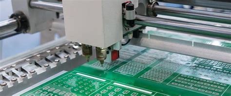
3.7 Design for Manufacturability (DFM)
Design for manufacturability (DFM) is an important consideration in high-speed PCB design. The design must be optimized for the manufacturing process to ensure that the final product meets the required specifications. This includes considerations such as trace width and spacing, via size and placement, and the selection of materials. Collaboration with the PCB manufacturer is essential to ensure that the design can be reliably produced.
4. Advanced Techniques in High-Speed PCB Design
As the demand for higher performance and faster data rates continues to grow, advanced techniques are being developed to address the challenges of high-speed PCB design.
4.1 Differential Pair Routing
Differential pair routing is commonly used in high-speed PCB design to transmit high-speed signals with minimal noise and crosstalk. Differential pairs consist of two traces that carry equal and opposite signals, which cancel out common-mode noise. Proper routing of differential pairs, including maintaining consistent spacing and length matching, is essential for ensuring signal integrity.
4.2 SerDes Technology
Serializer/Deserializer (SerDes) technology is widely used in high-speed communication systems to transmit data over high-speed serial links. SerDes devices convert parallel data into serial data for transmission and vice versa. Designing PCBs for SerDes technology requires careful consideration of signal integrity, impedance matching, and power integrity to ensure reliable data transmission at high speeds.
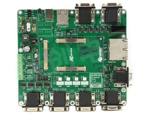
4.3 High-Speed Connectors and Interfaces
High-speed connectors and interfaces, such as PCIe, USB, and HDMI, are critical components in high-speed PCBs. These connectors must be carefully selected and placed to minimize signal degradation and ensure reliable connections. The design of the PCB must account for the electrical characteristics of the connectors, including impedance matching and signal routing.
4.4 Advanced Materials
The choice of PCB materials is critical in high-speed design. Advanced materials with low dielectric loss and high thermal conductivity are often used to improve signal integrity and thermal management. Materials such as Rogers, Isola, and Panasonic Megtron are commonly used in high-speed PCBs to achieve the desired performance.
4.5 3D Electromagnetic Simulation
3D electromagnetic simulation is an advanced technique used to analyze the behavior of high-speed signals on PCBs. These simulations can provide detailed insights into signal integrity, EMI, and power integrity, allowing designers to optimize the layout and routing of high-speed signals. Tools such as ANSYS HFSS and CST Studio Suite are commonly used for 3D electromagnetic simulation.
5. Conclusion
High-speed PCB design is a complex and challenging field that requires a deep understanding of signal integrity, power integrity, EMC, and thermal management. As the demand for faster and more efficient electronic systems continues to grow, the importance of high-speed PCB design will only increase. By following best practices and leveraging advanced techniques, engineers and designers can create high-speed PCBs that meet the performance and reliability requirements of modern electronic systems.
In summary, high-speed PCB design is a multidisciplinary endeavor that combines electrical engineering, materials science, and thermal management. The principles, challenges, and best practices discussed in this article provide a foundation for designing high-speed PCBs that can handle the demands of today’s high-frequency applications. As technology continues to evolve, staying abreast of the latest developments in high-speed PCB design will be essential for engineers and designers working in this dynamic field.