High-speed PCB design series basic knowledge 62 | General Checklist inspection
The last issue explained the common DRC and correction methods in PCB design. This issue introduces what aspects are included in the general Checklist inspection.
1 Netlist comparison
Confirm the report output by the netlist comparison tool to ensure that the netlist is consistent with the PCB board.
The final board imports the latest schematic to see the viewlog file to ensure that there are no other changes.
2 Structural inspection
Check whether the board frame and board thickness information of the single board are correct, and pay attention to whether there are gaps in special devices such as optical modules.
Check whether the height limit of the single board is correct. The height of the device under the radiator should be less than the minimum height of the BGA under the radiator -0.5mm or confirm the specific height limit value with the hardware and process.
Whether there are super-high devices under the anti-pad fiber outlet and the fiber path. Execute Auxitools/check/Height review select to check whether the device is super-high. Execute Auxitools/check/Height no height to check the device without height information, and find the device data to confirm whether it is super-high.
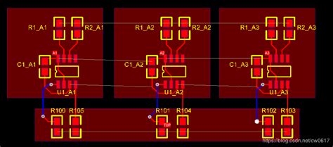
Check the number of single board positioning apertures, whether the holes are metallized and consistent with the structure diagram, and check the single board positioning device coding and the structure diagram
Check that the structure diagram is completely consistent with the PCB positioning device layout, the order of positioning devices (connectors, panel indicators, etc.), the position direction (gusset connector) is consistent with the structure diagram, and the engineering
requirements form. Positioning deviations within 1mil are prompt problems, deviations of 1mil are general problems, and deviations of more than 1mil are serious problems
Confirm that the cross silk screens of the optical module package and the shielding cover package overlap correctly. Note: Radiators, gusset connectors, etc. use standard packages
Whether the layout and wiring meet the requirements of the structural forbidden area, all forbidden areas and OPEN WINDOW areas inside the single board are drawn with Keepout.
Check whether there are traces, copper foil, silk screen or pads in the thin-wash area
Check the screw hole Top and Bottom layer pads within 0.5mm depth below the surface layer. Do not place non-ground signals and vias

3 Silk screen inspection
Execute the auxitools/check/refdes check… command to check and confirm each item one by one. If there is no auxiliary tool, check one by one. Check the silk screen direction, interference between silk screens, and soldermask on the silk screen to check whether the device frame, pin markings, polarity markings, etc. are on the pads or test points; whether the pin markings and polarity markings are ok;
The rated current and voltage values of the fuse have been added as required, for example: F1 T4AH/250V
The direction of the silk screen marking manually added to the single board is correct, focus on checking the silk screen on the back, and it is recommended to add silk screen manually for more than 6mil
The device label is kept at a minimum distance of 20mil from the board edge
Whether the device silk screen frame position number is lost
4 Safety review
The circuit in the 48V/BGND area meets the safety requirements, and focus on checking the main circuit.
The 48V area meets the following requirements:
- The distance requirements from the hole edge to the hole edge, and from the hole edge to the line edge: 2.1mm for the outer layer and 1.75mm for the inner layer in front of the fuse tube; 2.1mm for the outer layer and 0.75mm for the inner layer in the back of the fuse tube;
- The distance requirements from the line edge to the line edge: 2.0mm for the outer layer and 1.4mm for the inner layer in front of the fuse tube; 2.0mm for the outer layer and 0.4mm for the inner layer in the back of the fuse tube. Tip: There is no mandatory requirement for the back of the fuse tube, and it is recommended that the surface and inner layers are greater than 30mil.
The high-voltage area and the low-voltage area meet the safety requirements before the fuse, and the fuse (230V system) needs to add a fuse warning label
The front and rear isolation area below the common mode inductor must meet more than 100mil
Cut off the thin and long copper foil Cut off the thin and long protrusions (fine line) in the copper foil
5.Special device processing
For devices with metal shells (metal handles, horizontal voltage regulators, ferrite inductors, crystal oscillators SX6-0705B, etc., all plug-in crystals and DPAK, etc.), 1.5mm is prohibited around.
1mm of components are prohibited around other SMD crystals, 0.5mm of vias are prohibited, and no vias are drilled under all crystals (including ground vias)
VIS-SI7356 devices on the power supply part of the single board, pay attention to check whether the copper foil of other networks avoids the routekeepout of the package itself; MOS tubes with SOT89 package cannot have vias drilled in the prohibited area
It is necessary to ensure that the width of the copper foil at both ends of the thermistor is consistent, otherwise it is easy to cause misjudgment
Non-ground vias are not allowed in the copper-plated area of the optical module shielding shell
There are vias on the pads, and whether the back of the pads are copper-plated and bright
When copper is laid in the network of densely spaced devices, the SOLD of the pads is opened in the middle of the copper foil