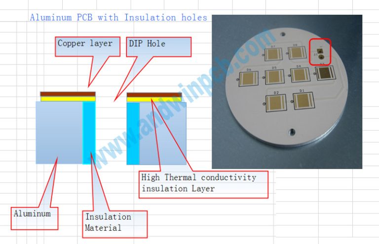
High speed pcb layout techniques
Optimizing Signal Integrity in High-Speed PCB Layouts
Optimizing signal integrity in high-speed PCB layouts is a critical aspect of modern electronic design, as it directly impacts the performance and reliability of the final product. As electronic devices continue to evolve, the demand for higher data rates and faster processing speeds necessitates meticulous attention to detail in PCB layout techniques. One of the primary considerations in high-speed PCB design is the management of signal integrity, which involves ensuring that signals are transmitted with minimal distortion and interference.
To begin with, the choice of materials plays a significant role in maintaining signal integrity.
High-frequency signals are particularly susceptible to losses and reflections, which can degrade performance. Therefore, selecting low-loss dielectric materials with stable electrical properties is essential. These materials help to minimize signal attenuation and ensure consistent impedance, which is crucial for high-speed signal transmission.
Another important factor is the layout of traces on the PCB.
The length, width, and spacing of traces must be carefully controlled to prevent signal degradation. For instance, longer traces can introduce delays and increase the likelihood of signal reflections, while narrower traces can lead to higher resistance and potential signal loss. To mitigate these issues, designers often use techniques such as controlled impedance routing and differential pair routing. Controlled impedance routing involves designing traces with specific impedance values to match the source and load, thereby reducing reflections and ensuring signal integrity. Differential pair routing, on the other hand, involves routing two complementary signals together, which helps to cancel out noise and reduce electromagnetic interference (EMI).
In addition to trace layout, the placement of components is another critical aspect of high-speed PCB design.
Components should be strategically placed to minimize the length of high-speed signal paths and reduce the potential for crosstalk and EMI. Placing components too close together can lead to signal coupling, where signals from one trace interfere with those on an adjacent trace. To avoid this, designers often use techniques such as ground planes and shielding. Ground planes provide a low-impedance return path for signals, which helps to reduce noise and improve signal integrity. Shielding, on the other hand, involves placing conductive barriers around sensitive components or traces to protect them from external interference.
Furthermore, power integrity is closely related to signal integrity in high-speed PCB layouts.
Ensuring a stable power supply is essential for maintaining signal quality. Power distribution networks (PDNs) must be designed to provide clean and stable power to all components, with minimal noise and voltage fluctuations. This can be achieved through the use of decoupling capacitors, which help to filter out noise and provide a stable voltage supply. Additionally, careful routing of power and ground traces, as well as the use of multiple power and ground planes, can help to reduce noise and improve overall power integrity.
Thermal management is another important consideration in high-speed PCB design.
High-speed components often generate significant amounts of heat, which can affect signal integrity and overall performance. Effective thermal management techniques, such as the use of thermal vias, heat sinks, and proper airflow design, are essential to dissipate heat and maintain optimal operating conditions.
In conclusion, optimizing signal integrity in high-speed PCB layouts requires a comprehensive approach that encompasses material selection, trace layout, component placement, power integrity, and thermal management. By carefully considering these factors and employing advanced design techniques, designers can ensure that their high-speed PCBs deliver reliable and high-performance operation in even the most demanding applications.
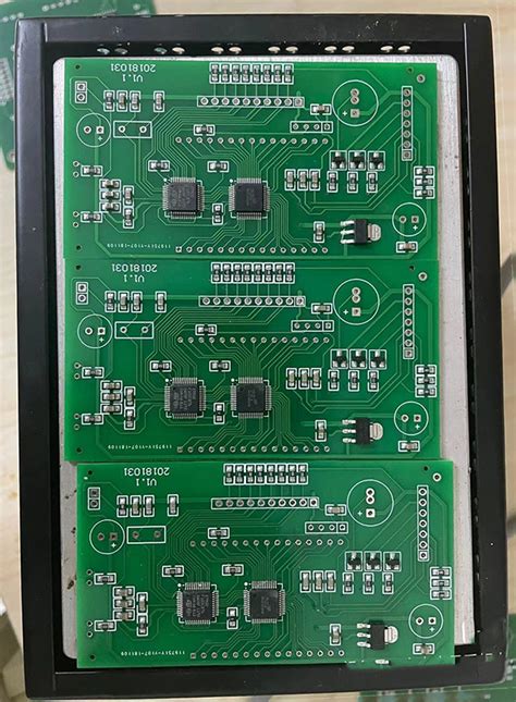
Effective Layer Stackup Strategies for High-Speed PCBs
Effective layer stackup strategies are crucial for the successful design of high-speed printed circuit boards (PCBs). As electronic devices continue to evolve, the demand for higher speeds and greater functionality has necessitated more sophisticated PCB designs. One of the most critical aspects of these designs is the layer stackup, which directly impacts signal integrity, electromagnetic compatibility (EMC), and overall performance.
To begin with, understanding the fundamental principles of layer stackup is essential.
A well-designed stackup minimizes signal loss, reduces electromagnetic interference (EMI), and ensures that the PCB can handle high-speed signals without degradation. Typically, high-speed PCBs consist of multiple layers, including signal layers, power planes, and ground planes. The arrangement and number of these layers depend on the complexity and requirements of the specific application.
One effective strategy for high-speed PCB layer stackup is to use a symmetrical structure.
Symmetry helps to balance the mechanical stresses during the manufacturing process, reducing the risk of warping and ensuring consistent performance. For instance, a common approach is to place signal layers between power and ground planes. This configuration not only provides a stable reference for signal transmission but also helps to contain EMI within the PCB, thereby improving EMC performance.
Moreover, the placement of power and ground planes is critical.
Ideally, these planes should be adjacent to each other, separated by a thin dielectric layer. This close proximity creates a low-inductance path, which is beneficial for high-speed signal return currents. Additionally, it helps to decouple the power supply, reducing noise and improving signal integrity. In some cases, designers may opt for multiple ground planes to further enhance performance, especially in designs with very high-speed signals.
Another important consideration is the dielectric material used between the layers.
The choice of dielectric material affects the impedance of the signal traces and the overall performance of the PCB. High-speed designs often require materials with low dielectric constant (Dk) and low dissipation factor (Df) to minimize signal loss and ensure reliable signal transmission. Furthermore, the thickness of the dielectric layers should be carefully controlled to maintain consistent impedance and avoid signal reflections.
Transitioning to the topic of signal routing, it is essential to maintain controlled impedance throughout the PCB.
Controlled impedance ensures that the signal traces have a consistent characteristic impedance, which is crucial for high-speed signal integrity. This can be achieved by carefully designing the trace width, spacing, and the distance to the reference planes. Additionally, differential pairs, which are commonly used in high-speed designs, should be routed with consistent spacing and length to maintain signal integrity and minimize skew.
In addition to these strategies, it is also important to consider the overall stackup height.
A thinner PCB can reduce the distance between layers, which is beneficial for high-speed signal transmission. However, it is essential to balance this with the mechanical strength and manufacturability of the PCB. Therefore, designers must carefully evaluate the trade-offs and select an appropriate stackup height that meets both electrical and mechanical requirements.
In conclusion, effective layer stackup strategies are vital for the successful design of high-speed PCBs. By employing a symmetrical structure, optimizing the placement of power and ground planes, selecting appropriate dielectric materials, and maintaining controlled impedance, designers can ensure that their PCBs meet the demanding requirements of high-speed applications. These strategies not only enhance signal integrity and EMC performance but also contribute to the overall reliability and functionality of the final product.
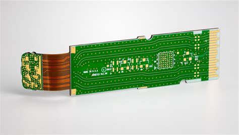
Managing Crosstalk in High-Speed PCB Designs
Managing crosstalk in high-speed PCB designs is a critical aspect of ensuring signal integrity and overall system performance. As electronic devices continue to evolve, the demand for higher speeds and greater functionality has led to increasingly complex PCB layouts. Crosstalk, which refers to the unwanted coupling of signals between adjacent traces, can significantly degrade the performance of high-speed circuits. Therefore, understanding and implementing effective techniques to manage crosstalk is essential for any PCB designer.
One of the primary strategies for managing crosstalk is to maintain adequate spacing between signal traces.
By increasing the distance between traces, the capacitive and inductive coupling that causes crosstalk can be minimized. This approach is particularly important for high-speed signals, where even small amounts of interference can lead to significant signal degradation. Additionally, designers should consider the use of differential pairs, which involve routing two complementary signals close together. This technique helps to cancel out any noise that may be induced, thereby reducing the impact of crosstalk.
Another effective method for mitigating crosstalk is to employ proper grounding techniques.
A well-designed ground plane can provide a low-impedance return path for signals, which helps to reduce the potential for crosstalk. Ensuring that the ground plane is continuous and free of interruptions is crucial, as any gaps or splits can create impedance discontinuities that exacerbate crosstalk issues. Furthermore, the use of ground vias strategically placed near signal vias can help to maintain signal integrity by providing a direct return path for high-frequency currents.
Shielding is another technique that can be employed to manage crosstalk in high-speed PCB designs.
By placing a grounded shield trace between two signal traces, the coupling between them can be significantly reduced. This approach is particularly useful in situations where it is not possible to increase the spacing between traces due to layout constraints. However, it is important to note that shielding can increase the overall complexity of the PCB design and may require additional layers, which can impact the cost and manufacturability of the board.
In addition to these physical layout techniques, careful consideration of signal routing is essential for managing crosstalk.
Avoiding long parallel runs of high-speed traces can help to minimize the potential for crosstalk. Instead, designers should aim to route traces at right angles to each other whenever possible. This approach helps to reduce the coupling between traces by minimizing the length of parallel segments. Additionally, the use of serpentine routing, where traces are intentionally meandered, can help to equalize the lengths of differential pairs and reduce the impact of crosstalk.
Finally, the selection of appropriate materials and stack-up configurations can play a significant role in managing crosstalk.
High-speed PCB designs often require the use of low-loss dielectric materials, which can help to reduce signal attenuation and maintain signal integrity. Additionally, a well-planned stack-up configuration that includes multiple ground and power planes can help to isolate high-speed signals and reduce the potential for crosstalk.
In conclusion, managing crosstalk in high-speed PCB designs requires a comprehensive approach that includes careful consideration of trace spacing, grounding techniques, shielding, signal routing, and material selection. By implementing these strategies, designers can effectively mitigate the impact of crosstalk and ensure the reliable performance of high-speed electronic systems. As technology continues to advance, the importance of managing crosstalk will only become more critical, making it essential for PCB designers to stay informed about the latest techniques and best practices in this field.
Techniques for Minimizing Electromagnetic Interference in High-Speed PCBs
In the realm of high-speed printed circuit board (PCB) design, minimizing electromagnetic interference (EMI) is paramount to ensuring optimal performance and reliability. As electronic devices become more sophisticated and operate at higher frequencies, the potential for EMI increases, necessitating the implementation of advanced techniques to mitigate its effects. One fundamental approach to reducing EMI in high-speed PCBs is through meticulous component placement. By strategically positioning components, designers can minimize the length of high-speed signal traces, thereby reducing the potential for radiated emissions. Placing high-speed components close to their corresponding connectors and ensuring that sensitive analog components are isolated from noisy digital components can significantly diminish EMI.
In addition to component placement, the use of proper grounding techniques is crucial.
A solid ground plane can act as a shield, absorbing and redirecting electromagnetic waves away from sensitive circuitry. Ensuring that the ground plane is continuous and unbroken helps maintain a low impedance path for return currents, which is essential for minimizing EMI. Furthermore, employing multiple ground planes in a multilayer PCB design can provide additional shielding and further reduce electromagnetic interference.
Another effective technique for minimizing EMI is the careful routing of signal traces.
High-speed signal traces should be kept as short and direct as possible to reduce the potential for radiated emissions. Additionally, differential pair routing can be employed for high-speed signals, as it helps cancel out electromagnetic fields generated by the signals, thereby reducing EMI. It is also advisable to route high-speed traces on internal layers of the PCB, sandwiched between ground planes, to provide additional shielding and minimize the potential for radiated emissions.
The use of decoupling capacitors is another critical technique for mitigating EMI in high-speed PCBs.
These capacitors help filter out high-frequency noise and provide a stable power supply to the components. Placing decoupling capacitors as close as possible to the power pins of integrated circuits (ICs) ensures that high-frequency noise is effectively filtered out before it can propagate through the PCB. Additionally, using a combination of capacitors with different values can provide effective filtering across a wide range of frequencies.
Moreover, the implementation of proper PCB stack-up design can play a significant role in minimizing EMI.
A well-designed stack-up can provide effective isolation between high-speed signal layers and power/ground planes, reducing the potential for crosstalk and radiated emissions. For instance, placing a ground plane adjacent to a high-speed signal layer can provide effective shielding and reduce the potential for EMI. Additionally, maintaining a consistent impedance throughout the PCB stack-up can help ensure signal integrity and minimize the potential for electromagnetic interference.
Lastly, the use of electromagnetic shielding can be an effective technique for minimizing EMI in high-speed PCBs.
Shielding can be implemented at both the PCB level and the enclosure level. At the PCB level, metal shields can be placed over sensitive components or high-speed signal traces to provide additional protection against electromagnetic interference. At the enclosure level, conductive coatings or metal enclosures can be used to shield the entire PCB from external electromagnetic fields.
In conclusion, minimizing electromagnetic interference in high-speed PCBs requires a comprehensive approach that encompasses various design techniques. By carefully considering component placement, grounding techniques, signal trace routing, decoupling capacitors, PCB stack-up design, and electromagnetic shielding, designers can effectively mitigate EMI and ensure the optimal performance and reliability of high-speed electronic devices. As technology continues to advance and operating frequencies increase, the importance of these techniques will only become more critical in the pursuit of high-performance PCB designs.

