High speed signal pcb design
There are many sources for high speed signal PCB design, including:
1. Altium Designer: A popular PCB design software that offers high speed signal design capabilities.
2. Cadence Allegro: A comprehensive PCB design software that includes high speed signal design features.
3. Mentor Graphics PADS: A PCB design software that includes high speed signal design capabilities.
4. ANSYS HFSS: A simulation software that can be used for high speed signal design analysis.
5. Signal Integrity Journal: An online resource for high speed signal design information, including articles, webinars, and white papers.
6. IEEE Transactions on Microwave Theory and Techniques: A peer-reviewed journal that publishes research on high speed signal design.
7. High Speed Digital Design: A book by Howard Johnson and Martin Graham that provides a comprehensive guide to high speed signal design.
8. Texas Instruments: A semiconductor company that offers resources and tools for high speed signal design, including application notes, reference designs, and evaluation boards.
9. Keysight Technologies: A company that offers test and measurement equipment for high speed signal design, including oscilloscopes, signal generators, and network analyzers.
10. Samtec: A company that offers high speed signal connectors and cables for PCB design.

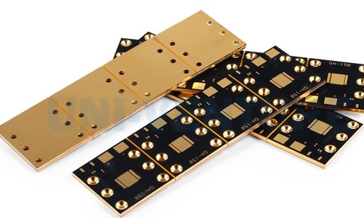
High speed signal PCB design refers to the process of designing printed circuit boards (PCBs) that are optimized for transmitting high frequency signals with minimal distortion and loss.
This type of design is typically required for applications such as telecommunications, data communication, and high-speed digital circuits.

To achieve high speed signal performance, the following design considerations must be taken into account:
1. Signal integrity:
The PCB must be designed to minimize signal distortion and loss.
This can be achieved by controlling the impedance of the transmission lines, minimizing crosstalk between traces,
and reducing the parasitic capacitance and inductance of the circuit.
2. Grounding:
Proper grounding is essential for high speed signal performance.
The PCB must have a solid ground plane and the signal traces must be routed over it to minimize noise and interference.
3. Power distribution:
The PCB must have a well-designed power distribution network to ensure stable and clean power delivery to the components.
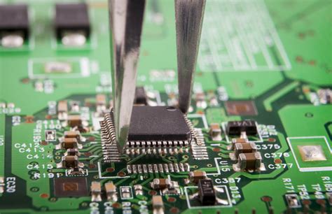
4. Component placement:
The placement of components on the PCB can have a significant impact on signal performance.
Components that generate noise or interfere with the signal should be placed away from high speed signal traces.
5. Routing:
The routing of high speed signal traces must be carefully planned to minimize signal distortion and loss.
Trace lengths should be matched to ensure consistent signal timing, and vias should be minimized to reduce signal reflection.
Overall, high speed signal PCB design requires careful planning, attention to detail, and a thorough understanding of signal integrity principles.