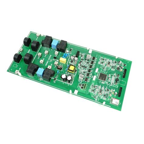
High speed usb pcb layout recommendations
Optimizing Trace Width and Spacing for High-Speed USB Signals
In the realm of high-speed USB design, optimizing trace width and spacing is crucial to ensure signal integrity and minimize electromagnetic interference. As USB technology continues to evolve, with standards such as USB 3.0 and USB 3.1 offering data transfer rates of up to 10 Gbps, the importance of meticulous printed circuit board (PCB) layout cannot be overstated. To achieve optimal performance, designers must consider several factors, including impedance control, crosstalk reduction, and signal reflection minimization.
To begin with, maintaining the correct impedance is essential for high-speed USB signals.
Typically, USB traces are designed to have a characteristic impedance of 90 ohms differential. This requires careful calculation of trace width and spacing, taking into account the dielectric constant of the PCB material and the thickness of the copper layers. By ensuring that the impedance is consistent along the entire length of the trace, designers can prevent signal reflections that may lead to data corruption. Moreover, using simulation tools to model the impedance can provide valuable insights and help in fine-tuning the layout.
In addition to impedance control, reducing crosstalk is another critical consideration.
Crosstalk occurs when signals from adjacent traces interfere with each other, potentially causing data errors. To mitigate this, it is advisable to maintain adequate spacing between high-speed USB traces and other signal lines. A general rule of thumb is to keep a minimum spacing of three times the trace width between differential pairs and other signals. This spacing helps to minimize electromagnetic coupling and ensures that the integrity of the USB signals is preserved.
Furthermore, the use of ground planes plays a significant role in optimizing trace width and spacing.
Ground planes provide a return path for signals and help to shield traces from external noise sources. By placing USB traces over a continuous ground plane, designers can enhance signal integrity and reduce the risk of electromagnetic interference. Additionally, stitching vias can be employed to connect the ground planes on different layers, further improving the shielding effectiveness.
Another important aspect to consider is the routing of differential pairs.
Differential signaling is a common technique used in high-speed USB design to improve noise immunity. When routing differential pairs, it is crucial to maintain equal trace lengths to prevent skew, which can lead to timing mismatches and data errors. Designers should aim to match the lengths of the positive and negative traces as closely as possible, using serpentine routing if necessary to achieve this balance.
Moreover, avoiding sharp bends in the traces is advisable, as these can cause impedance discontinuities and signal reflections.
Instead, gentle curves or 45-degree angles should be used to maintain a smooth transition along the trace path. This approach helps to preserve the integrity of the high-speed signals and reduces the likelihood of performance degradation.
In conclusion, optimizing trace width and spacing for high-speed USB signals is a multifaceted task that requires careful consideration of various design parameters. By focusing on impedance control, crosstalk reduction, and proper routing techniques, designers can ensure that their PCB layouts support the high data transfer rates demanded by modern USB standards. Through meticulous planning and the use of advanced simulation tools, it is possible to achieve a robust and reliable high-speed USB design that meets the stringent requirements of today’s technology landscape.
Effective Ground Plane Strategies in High-Speed USB PCB Design
In the realm of high-speed USB PCB design, the implementation of effective ground plane strategies is paramount to ensuring optimal performance and signal integrity. As data transfer rates continue to escalate, the challenges associated with maintaining signal quality and minimizing electromagnetic interference (EMI) become increasingly complex. Therefore, understanding and applying sound ground plane strategies is essential for engineers tasked with designing high-speed USB circuits.
To begin with, the ground plane serves as a reference point for all signals on the PCB, providing a return path for current and helping to minimize noise.
In high-speed USB designs, a continuous and unbroken ground plane is crucial. This continuity helps to reduce impedance discontinuities, which can lead to signal reflections and degradation. By maintaining a solid ground plane, designers can ensure that the return path for high-speed signals is as short and direct as possible, thereby minimizing the potential for signal integrity issues.
Moreover, the placement of the ground plane in relation to signal traces is a critical consideration.
Ideally, high-speed signal traces should be routed on a layer adjacent to the ground plane. This proximity helps to create a controlled impedance environment, which is vital for maintaining signal integrity at high frequencies. Additionally, the use of microstrip or stripline configurations can further enhance the performance of high-speed USB signals by providing a well-defined transmission line structure.
Transitioning to the topic of via placement, it is important to recognize that vias can introduce inductance and capacitance, which may adversely affect high-speed signals.
To mitigate these effects, designers should minimize the number of vias in high-speed signal paths and ensure that any necessary vias are placed strategically. For instance, stitching vias can be used to connect the ground planes of different layers, thereby reducing loop inductance and improving the overall performance of the PCB.
Furthermore, the concept of ground plane segmentation warrants careful consideration.
While it may be tempting to segment the ground plane to isolate different functional areas of the PCB, this practice can lead to unintended consequences in high-speed designs. Segmentation can create impedance discontinuities and increase the risk of EMI. Therefore, it is generally advisable to maintain a continuous ground plane and use other methods, such as careful component placement and shielding, to manage noise and interference.
In addition to these strategies, the use of decoupling capacitors is another effective technique for enhancing ground plane performance.
By placing decoupling capacitors close to power pins, designers can help to stabilize the power supply and reduce noise on the ground plane. This practice is particularly important in high-speed USB designs, where power integrity is closely linked to signal integrity.
In conclusion, effective ground plane strategies are a cornerstone of successful high-speed USB PCB design. By maintaining a continuous ground plane, optimizing the placement of signal traces and vias, and employing decoupling techniques, designers can significantly enhance the performance and reliability of their circuits. As data rates continue to rise, the importance of these strategies will only grow, underscoring the need for engineers to remain vigilant and informed about the latest developments in PCB design practices. Through careful planning and execution, it is possible to overcome the challenges associated with high-speed USB design and achieve superior signal integrity and performance.
Minimizing Signal Integrity Issues in High-Speed USB Layouts
In the realm of high-speed USB design, ensuring signal integrity is paramount to achieving optimal performance and reliability. As data rates increase, the challenges associated with maintaining signal integrity become more pronounced, necessitating meticulous attention to the printed circuit board (PCB) layout. To minimize signal integrity issues in high-speed USB layouts, several key recommendations should be considered, each contributing to the overall robustness of the design.
Firstly, it is essential to focus on the trace routing of the USB differential pairs.
Differential signaling is a fundamental aspect of high-speed USB communication, and maintaining the integrity of these signals is crucial. To achieve this, designers should ensure that the differential pairs are routed symmetrically and with consistent trace widths and spacing. This uniformity helps to maintain the characteristic impedance, which is typically 90 ohms for USB 2.0 and 85 ohms for USB 3.0 and beyond. Deviations from these impedance values can lead to reflections and signal degradation, thus impacting performance.
Moreover, minimizing the length of the differential pairs is another critical consideration.
Longer trace lengths can introduce additional parasitic inductance and capacitance, which can adversely affect signal quality. When longer traces are unavoidable, it is advisable to employ techniques such as serpentine routing to equalize the lengths of the differential pairs, thereby preserving signal timing and reducing skew.
In addition to trace routing, the placement of components plays a significant role in minimizing signal integrity issues.
Placing USB connectors and associated components as close as possible to the edge of the PCB can reduce trace lengths and potential interference from other board elements. Furthermore, careful attention should be paid to the placement of decoupling capacitors. These components should be positioned close to the power pins of the USB controller to provide effective noise suppression and ensure stable power delivery.
Grounding is another critical aspect of high-speed USB PCB layout.
A solid ground plane is essential for providing a low-impedance return path for high-frequency signals, thereby reducing electromagnetic interference (EMI) and crosstalk. It is advisable to avoid splitting the ground plane under the differential pairs, as this can disrupt the return path and degrade signal integrity. Additionally, stitching vias should be used to connect different ground layers, ensuring a continuous ground path across the PCB.
Transitioning to the topic of vias, it is important to minimize their use in high-speed USB layouts.
Vias introduce inductance and capacitance, which can distort high-frequency signals. When vias are necessary, it is beneficial to use back-drilled or blind vias to reduce their impact on signal integrity. Furthermore, ensuring that vias are placed symmetrically on differential pairs can help maintain balance and reduce skew.
Finally, signal integrity can be further enhanced by employing proper termination techniques.
Termination resistors should be placed as close as possible to the receiver to match the characteristic impedance of the transmission line, thereby minimizing reflections. Additionally, the use of common-mode chokes can help suppress common-mode noise, further improving signal quality.
In conclusion, minimizing signal integrity issues in high-speed USB layouts requires a comprehensive approach that encompasses trace routing, component placement, grounding, via management, and termination techniques. By adhering to these recommendations, designers can significantly enhance the performance and reliability of high-speed USB systems, ensuring that they meet the demands of modern applications.
Best Practices for Via Placement in High-Speed USB PCBs
When designing high-speed USB printed circuit boards (PCBs), careful consideration of via placement is crucial to ensure signal integrity and optimal performance. Vias, which are conductive pathways that allow signals to pass between different layers of a PCB, can significantly impact the electrical characteristics of high-speed signals. Therefore, understanding best practices for via placement is essential for engineers aiming to design efficient and reliable USB PCBs.
To begin with, it is important to minimize the number of vias used in high-speed USB signal paths.
Each via introduces a small amount of inductance and capacitance, which can degrade signal quality by causing reflections and impedance mismatches. By reducing the number of vias, designers can maintain a more consistent impedance profile along the signal path, thereby enhancing signal integrity. However, when vias are unavoidable, it is advisable to use them judiciously and strategically.
In addition to minimizing via count, the placement of vias should be carefully considered to avoid disrupting the signal path.
Ideally, vias should be placed symmetrically with respect to differential pairs, such as those used in USB data lines. This symmetry helps maintain the balance of the differential signals, reducing the potential for common-mode noise and ensuring that the signals remain tightly coupled. Furthermore, when routing differential pairs through vias, it is beneficial to keep the via stubs as short as possible. Via stubs, which are the unused portions of a via, can act as antennas, radiating unwanted electromagnetic interference (EMI) and affecting signal quality. By employing back-drilling techniques or using blind or buried vias, designers can effectively minimize the length of via stubs.
Moreover, the aspect ratio of vias, defined as the ratio of the via’s length to its diameter, should be optimized to reduce parasitic effects.
A lower aspect ratio is generally preferred, as it results in lower inductance and capacitance. This can be achieved by selecting appropriate via sizes and ensuring that the PCB stack-up is designed to accommodate these dimensions. Additionally, using via-in-pad technology, where vias are placed directly within the pads of surface-mounted components, can help reduce the overall length of the signal path and improve signal integrity.
Transitioning to the topic of via shielding, it is worth noting that placing ground vias adjacent to signal vias can provide effective shielding against EMI.
This technique, known as via stitching, involves connecting multiple ground vias around the signal vias to create a low-impedance return path for high-frequency signals. By doing so, designers can mitigate crosstalk and reduce the susceptibility of the signal traces to external noise sources. Furthermore, via stitching can enhance the mechanical stability of the PCB, which is particularly beneficial in high-speed applications where mechanical stress can impact performance.
Finally, it is essential to consider the thermal implications of via placement in high-speed USB PCBs.
Vias can serve as thermal conduits, facilitating heat dissipation from components to the PCB’s ground plane. By strategically placing thermal vias near heat-generating components, designers can improve thermal management and prevent overheating, which can adversely affect the performance and reliability of the USB interface.
In conclusion, the placement of vias in high-speed USB PCBs is a critical aspect of design that requires careful attention to detail. By minimizing via count, optimizing via placement, and considering factors such as aspect ratio, shielding, and thermal management, engineers can enhance signal integrity and ensure the reliable operation of high-speed USB interfaces. Through these best practices, designers can effectively address the challenges associated with via placement and achieve superior performance in their USB PCB designs.


