High Temperature PCBs – Circuit Boards for High Temperature Applications
It’s no secret that designers are squeezing more performance out of printed circuit boards. Power densities are rising, and with them come higher temperatures that can wreak havoc on conductors and dielectrics. Increased temperatures – whether from I2R losses or environmental factors – affect thermal and electrical impedance, leading to erratic system performance, if not outright failure.
Differences in the rates of thermal expansion (a measure of a material’s tendency to expand when heated and contract when cooled) between conductors and dielectrics can create mechanical stresses that can lead to cracking and connection failures, especially if the board is subjected to cyclic heating and cooling. If temperatures get high enough, the dielectric can completely lose its structural integrity, knocking over the first domino in a cascade of trouble.
Heat has always been a factor in PCB performance, and designers are accustomed to incorporating heat sinks into their PCBs, but the demands of today’s high power density designs often overwhelm traditional PCB thermal management practices.
Mitigating the effects of high temperatures has far-reaching implications, not only on the performance and reliability of high-temperature PCBs, but also on factors such as:
Component (or system) weight
Application size
Cost
Power requirements
A high-temperature circuit board is generally defined as one with a Tg (glass transition temperature) above 170°C.
For continuous heat loads operating about 25°C below Tg, high-temperature PCBs should follow a simple rule of thumb.
This means that if your product is in the 130°C range or higher, a high-Tg material is recommended.
The most common high-Tg materials include:
- ISOLA IS410
- ISOLA IS420
- ISOLA G200
- Shengyi S1000-2
-ITEQ IT-180A
- ARLON 85N
In this article, we will discuss some design methods and techniques used in high-temperature PCB manufacturing and PCB assembly to help designers cope with high-temperature applications.
PCB Thermal Dissipation Techniques and Design Considerations
Heat is dissipated through one or more mechanisms – radiation, convection, conduction – and the design team must keep all three in mind when deciding how to manage system and component temperatures.
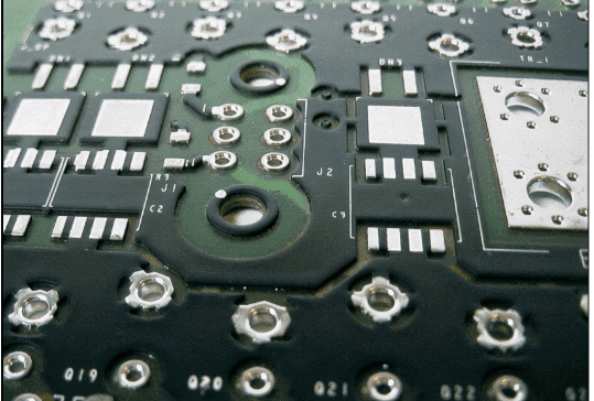
Heavy Copper PCBs
Radiation
- Radiation emits energy in the form of electromagnetic waves. We tend to think of it as just things that emit light, but the fact is that anything with a temperature above absolute zero radiates heat energy.
- While radiated heat usually has minimal impact on board performance, sometimes it can be the straw that breaks the camel’s back. To effectively remove heat, electromagnetic waves should have a relatively clear path away from their source.
- Reflective surfaces impede the outflow of photons, causing a large number of them to return to their source. If by unfortunate chance, the reflective surfaces work together to form a parabolic mirror effect, they can concentrate radiated energy from many sources and focus it on one inauspicious part of the system, causing real trouble.
Convection
- Convection is the transfer of heat to a fluid – air, water, etc. Some convection is “natural”: the fluid absorbs heat from the source, becomes less dense, rises from the source to the sink, cools, becomes more dense, returns to the source, and repeats the process. (Recall the “rain cycle” from grade school) Other convection is “forced” by a fan or pump.
- The key factors affecting convection are the temperature difference between the source and the coolant, how easily the source transfers heat, how easily the coolant absorbs the heat, the flow rate of the coolant, and the surface area over which the heat is transferred. Liquids absorb heat more easily than gases.
Conduction
Conduction is the transfer of heat through direct contact between a heat source and a heat sink. In many ways it is similar to electric current: the temperature difference between the source and sink is similar to voltage, the amount of heat transferred per unit time is similar to amperes, and the ease with which heat flows through a thermal conductor is similar to electrical conductance.
In fact, the factors that make for a good electrical conductor often also make for a good thermal conductor, since both represent forms of molecular or atomic motion. For example, copper and aluminum are both excellent conductors of both heat and electricity. Large conductor cross-sections improve the conductivity of both heat and electrons. As with electrical circuits, long, tortuous flow paths can severely reduce the efficiency of a conductor.
Typically, the primary mechanism for removing heat from a circuit board is by conduction to a suitable heat sink, where convection transfers the heat to the environment.
Some heat is dissipated and radiated directly from the source, but typically most of the heat is drawn away through specially designed channels called “thermal vias” or “thermal vias.” PCB heat sinks are relatively large, highly radiative, surfaces (often corrugated or finned to further increase surface area) bonded to a conductive (e.g., copper or aluminum) backing, a highly labor-intensive process.
PCB heat sinks may also be attached to the chassis of the device to utilize its surface area. Fans are typically used to provide the cooling air flow, and in extreme cases, the cooling air itself can be cooled in an air-to-liquid heat exchanger.
Multilayer Heat Plate
Ultimately, the thermal management options available to the designer are to reduce power density, remove or isolate the device from the heat source, provide a more robust cooling mechanism (e.g., larger fans, liquid cooling systems, etc.), increase the size and accessibility of the heat sink, use larger conductors, or use specialized materials that can withstand higher temperatures. All of this has an impact on the cost, size, and weight of the entire system and must be considered at the earliest concept development and design stages.

New Thermal Management Techniques
PCB manufacturers are well aware of the limitations of standard manufacturing practices and are striving to keep up with today’s design challenges by offering new PCBs designed for high temperatures. These PCBs all employ heavy copper circuits to increase current carrying capacity while reducing I2R losses, but the implementation can vary widely.
Increasingly, we are seeing “heavy copper” and “extreme copper” boards, which, as the description implies, use thicker, heavier copper layers than standard PCBs. If heavy (or extreme) copper is not needed everywhere, heavy copper circuits and standard copper circuits can be combined to allow both power and signal currents to be carried on a single board.
The process for manufacturing heavy/extreme copper PCBs is similar to that for standard PCBs, except for special etching and plating techniques. Advantages are greater current carrying capacity, lower I2R losses, increased mechanical strength, the ability to incorporate features such as efficient onboard heat sinks and onboard planar transformers, and reduced product size (due to the ability to combine heavy and standard circuitry on one board). Relatively low cost, since onboard heat sinks do not require the tedious manual fabrication of standard adhesive heat sinks.
A different approach is to embed heavy rectangular copper wires in place of heavy/extreme plated copper.
The advantages over standard PCBs are similar to those of heavy/extreme copper PCBs: ability to combine power and signal currents, reduced heating and improved heat dissipation, increased strength, elimination of connectors, reduced layer count, smaller overall system volume. Some claim that boards with embedded wires are easier to solder than thick copper boards, but this should be evaluated on a case-by-case basis.
Another thermal management technology that should be considered is computational fluid dynamics (CFD) software that can be integrated with standard PCB design packages, such as Mentor Graphics’ FloTherm PCB®.
As performance boundaries become harder and harder, the old rules of thumb and back-of-the-napkin thermal calculations become less reliable. In capable hands, a good CFD package—especially one designed specifically for PCB or electronics cooling applications—can eliminate much of the guesswork, increase design efficiency, avoid potentially costly mistakes, and reduce time to market.
Design and Development
Given all of the trade-offs described earlier, the design and development of a product must be shaped by a team that represents key stakeholders: customers, sales, and marketing, of course, but also customer service, procurement, manufacturing, and engineering. Suppliers with design-for-manufacturing and technical expertise, such as PCB manufacturers, must be integral members of the team; considerations of manufacturing, assembly, test, and service must be intrinsic, not add-on.
Techniques such as quality function deployment or TRIZ can be used to prioritize and reconcile competing design requirements, materials, and production technologies. First-pass cost-benefit analyses can be performed parametrically and then refined as actual costs become available. To minimize rollout problems, software such as Mentor Graphics’ “Valor MSS PCB” solution suite can be used to formulate, simulate, and improve manufacturing and test processes. The goal is frequent design iterations—creative failures, as they are known—that converge quickly to a final solution.
Although product requirements are becoming increasingly stringent, we have the tools, technologies, and methods to cope with them. Surviving in today’s competitive market requires us to adopt and adapt accordingly.


