High voltage pcb trace spacing
Importance Of Proper Trace Spacing In High Voltage PCB Design
In the realm of high voltage printed circuit board (PCB) design, the importance of proper trace spacing cannot be overstated. As electronic devices become increasingly complex and compact, ensuring the reliability and safety of these systems is paramount. One of the critical factors in achieving this is the meticulous consideration of trace spacing, particularly in high voltage applications. Proper trace spacing is essential to prevent electrical arcing, which can lead to catastrophic failures, including short circuits, component damage, and even fires. Therefore, understanding the principles and guidelines for trace spacing is crucial for engineers and designers working with high voltage PCBs.
To begin with, trace spacing refers to the distance between conductive traces on a PCB.
In high voltage applications, this spacing must be carefully calculated to withstand the potential difference between traces without allowing electrical discharge. The risk of arcing increases with higher voltages, making it imperative to adhere to industry standards and guidelines. The primary standard that governs trace spacing is the IPC-2221, which provides comprehensive guidelines for determining the appropriate spacing based on the voltage levels and environmental conditions. By following these standards, designers can ensure that their PCBs are both safe and reliable.
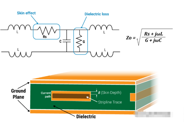
Moreover, the dielectric properties of the PCB material play a significant role in determining the necessary trace spacing.
Different materials have varying dielectric strengths, which influence their ability to insulate against high voltages. For instance, materials with higher dielectric constants can allow for closer trace spacing, while those with lower constants require greater distances to prevent breakdown. Consequently, selecting the appropriate PCB material is a critical step in the design process, as it directly impacts the trace spacing requirements.
In addition to material considerations, environmental factors such as humidity, temperature, and altitude can also affect trace spacing.
High humidity levels can reduce the dielectric strength of the air, increasing the likelihood of arcing. Similarly, elevated temperatures can cause materials to expand and potentially reduce the spacing between traces. At higher altitudes, the reduced air pressure can lower the breakdown voltage, necessitating greater trace spacing. Therefore, designers must account for these environmental conditions when determining the appropriate spacing for high voltage traces.
Furthermore, the consequences of inadequate trace spacing extend beyond safety concerns.
Insufficient spacing can lead to electromagnetic interference (EMI), which can disrupt the performance of the PCB and other nearby electronic devices. By ensuring proper trace spacing, designers can minimize EMI and enhance the overall functionality of the system. Additionally, maintaining adequate spacing can improve the thermal performance of the PCB by allowing for better heat dissipation, which is particularly important in high voltage applications where power levels are significant.
In conclusion, the importance of proper trace spacing in high voltage PCB design is multifaceted, encompassing safety, reliability, and performance considerations.
By adhering to established standards and guidelines, selecting appropriate materials, and accounting for environmental factors, designers can mitigate the risks associated with high voltage applications. As technology continues to advance, the demand for compact and efficient electronic devices will only increase, making the role of trace spacing in high voltage PCB design more critical than ever. Through careful planning and execution, engineers can ensure that their designs meet the rigorous demands of modern electronic systems, ultimately contributing to safer and more reliable technology.

Guidelines For Determining High Voltage PCB Trace Spacing
When designing printed circuit boards (PCBs) for high voltage applications, one of the critical considerations is determining the appropriate trace spacing. This aspect is crucial not only for ensuring the functionality of the board but also for maintaining safety and compliance with industry standards. High voltage PCB trace spacing refers to the distance between conductive traces on a PCB that carry high voltage signals. Proper spacing is essential to prevent electrical arcing, which can lead to circuit failure or even catastrophic damage.
To begin with, understanding the factors that influence trace spacing is vital.
The primary considerations include the voltage level, the environment in which the PCB will operate, and the materials used in the PCB’s construction. Higher voltages require greater spacing to prevent arcing and ensure reliable operation. Additionally, environmental factors such as humidity, altitude, and potential contamination can affect the required spacing. For instance, higher humidity levels can reduce the dielectric strength of air, necessitating increased spacing to prevent breakdown.
Moreover, the choice of materials plays a significant role in determining trace spacing.
Different PCB materials have varying dielectric properties, which influence their ability to withstand high voltages. For example, materials with higher dielectric constants can allow for reduced spacing, while those with lower constants may require increased distances between traces. Therefore, selecting the appropriate material is a crucial step in the design process.
Industry standards and guidelines provide a valuable framework for determining high voltage PCB trace spacing.
Organizations such as the IPC (Association Connecting Electronics Industries) offer standards like IPC-2221, which outlines general design requirements for PCBs, including trace spacing recommendations. These standards take into account various factors, including voltage levels and environmental conditions, to provide designers with a baseline for safe and effective PCB design.
In addition to adhering to industry standards, designers must also consider the specific requirements of their application.
For instance, in applications where space is limited, it may be necessary to optimize trace spacing while still ensuring safety and reliability. This can involve using advanced design techniques, such as incorporating guard traces or utilizing conformal coatings, to enhance the board’s performance without compromising safety.
Furthermore, simulation tools can be invaluable in the design process, allowing engineers to model and analyze the electrical behavior of their PCB designs under various conditions.
These tools can help identify potential issues related to trace spacing and provide insights into how different design choices may impact the board’s performance. By leveraging simulation, designers can make informed decisions and optimize their designs for high voltage applications.
In conclusion, determining the appropriate high voltage PCB trace spacing is a multifaceted process that requires careful consideration of various factors, including voltage levels, environmental conditions, and material properties. By adhering to industry standards and leveraging advanced design techniques and simulation tools, designers can ensure the safety and reliability of their high voltage PCBs. Ultimately, a well-designed PCB not only meets the functional requirements of the application but also adheres to safety standards, thereby minimizing the risk of electrical failure and enhancing the overall performance of the electronic system.
Common Mistakes In High Voltage PCB Trace Spacing And How To Avoid Them
In the realm of high voltage printed circuit board (PCB) design, trace spacing is a critical factor that can significantly impact the performance and safety of the final product. However, designers often make common mistakes in this area, which can lead to catastrophic failures or suboptimal performance. Understanding these pitfalls and learning how to avoid them is essential for anyone involved in high voltage PCB design.
One of the most frequent mistakes is underestimating the required spacing between traces.
High voltage applications demand greater spacing to prevent arcing and ensure safety. Designers sometimes rely on general PCB design rules without considering the specific requirements of high voltage applications. This oversight can lead to insufficient spacing, which increases the risk of electrical discharge and potential damage to the board. To avoid this, it is crucial to consult industry standards such as IPC-2221, which provides guidelines for determining appropriate trace spacing based on voltage levels.
Another common error is neglecting environmental factors that can influence trace spacing.
Factors such as humidity, altitude, and contamination can affect the dielectric properties of the PCB material, thereby impacting the necessary spacing. For instance, higher humidity levels can reduce the dielectric strength of the material, necessitating wider spacing to prevent breakdown. Designers should account for these environmental conditions during the design phase to ensure that the PCB will perform reliably under all expected operating conditions.
Moreover, designers often overlook the impact of manufacturing tolerances on trace spacing.
Variations in the etching process can lead to discrepancies between the designed and actual trace widths and spacings. If the design does not account for these tolerances, the final product may have traces that are too close together, increasing the risk of failure. To mitigate this risk, it is advisable to incorporate a margin of safety into the design, allowing for potential variations during manufacturing.
In addition to these technical considerations, communication breakdowns between design and manufacturing teams can also lead to spacing issues.
Designers may assume that manufacturers are aware of the specific requirements for high voltage applications, while manufacturers may not have the necessary information to adjust their processes accordingly. To prevent such misunderstandings, it is essential to maintain clear and open communication throughout the design and manufacturing process. Providing detailed documentation and specifications can help ensure that all parties are aligned and that the final product meets the necessary standards.
Furthermore, the use of inappropriate materials can exacerbate trace spacing problems.
Some materials may not have the required dielectric properties to support high voltage applications, leading to inadequate spacing and increased risk of failure. Selecting materials with suitable dielectric strength and thermal properties is crucial for maintaining proper trace spacing and ensuring the reliability of the PCB.
In conclusion, avoiding common mistakes in high voltage PCB trace spacing requires a comprehensive understanding of the factors that influence spacing requirements. By considering industry standards, environmental conditions, manufacturing tolerances, and material properties, designers can create PCBs that are both safe and effective. Additionally, fostering clear communication between design and manufacturing teams can help prevent misunderstandings and ensure that the final product meets all necessary specifications. By addressing these areas, designers can significantly reduce the risk of failure and enhance the performance of high voltage PCBs.
Innovations In High Voltage PCB Trace Spacing Techniques
In the realm of printed circuit board (PCB) design, the demand for high voltage applications has necessitated innovative approaches to trace spacing. As electronic devices become more sophisticated, the need for efficient and safe high voltage PCB trace spacing techniques has become increasingly critical. This evolution is driven by the dual imperatives of ensuring device reliability and maintaining user safety. Consequently, engineers and designers are continually exploring new methodologies to optimize trace spacing, thereby enhancing the performance and safety of high voltage PCBs.
One of the primary considerations in high voltage PCB design is the prevention of electrical arcing and short circuits.
To address this, designers must carefully calculate the appropriate spacing between conductive traces. Traditionally, the spacing is determined based on the voltage level, environmental conditions, and the dielectric properties of the PCB material. However, as voltage levels increase, the conventional methods of determining trace spacing may fall short, necessitating more advanced techniques.
Recent innovations in high voltage PCB trace spacing have focused on leveraging advanced materials and design software.
For instance, the use of high-performance dielectric materials can significantly enhance the insulation properties of a PCB, allowing for reduced trace spacing without compromising safety. These materials are engineered to withstand higher voltages and temperatures, providing a robust solution for modern high voltage applications. Additionally, the integration of sophisticated design software enables precise modeling and simulation of electrical fields, allowing designers to optimize trace spacing with greater accuracy.
Moreover, the advent of three-dimensional (3D) PCB design has opened new avenues for trace spacing optimization.
By utilizing 3D design techniques, engineers can create multi-layered PCBs that offer increased surface area for trace routing. This approach not only facilitates more efficient use of space but also allows for greater flexibility in trace spacing, particularly in high voltage applications where traditional two-dimensional designs may be limited. Furthermore, 3D design can help mitigate issues related to electromagnetic interference (EMI), which is a common concern in high voltage environments.
In addition to material and design innovations, regulatory standards play a crucial role in shaping high voltage PCB trace spacing techniques.
Organizations such as the International Electrotechnical Commission (IEC) and Underwriters Laboratories (UL) provide guidelines that dictate minimum trace spacing requirements based on voltage levels and environmental factors. Adhering to these standards is essential for ensuring the safety and reliability of high voltage PCBs. As these standards evolve, they continue to influence the development of new trace spacing methodologies.
Another promising area of innovation is the use of machine learning algorithms to predict optimal trace spacing configurations.
By analyzing vast datasets of PCB designs and their performance metrics, machine learning models can identify patterns and suggest trace spacing solutions that maximize efficiency and safety. This data-driven approach offers the potential to revolutionize high voltage PCB design by providing designers with insights that were previously unattainable through traditional methods.
In conclusion, the field of high voltage PCB trace spacing is undergoing significant transformation, driven by advancements in materials, design techniques, regulatory standards, and data analytics. As these innovations continue to evolve, they promise to enhance the safety, reliability, and performance of high voltage PCBs, meeting the ever-growing demands of modern electronic applications. Through a combination of cutting-edge technology and adherence to rigorous standards, the future of high voltage PCB trace spacing looks both promising and exciting.