How Advanced PCB Options Work and Their Benefits
Introduction
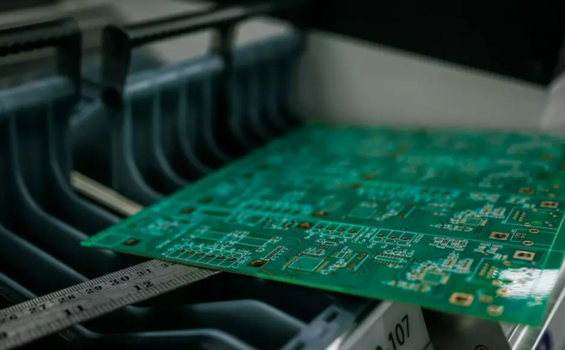
Printed Circuit Boards (PCBs) are the backbone of modern electronics, enabling the interconnection of components in devices ranging from smartphones to industrial machinery. As technology advances, so do PCB manufacturing techniques, leading to the development of advanced PCB options that enhance performance, reliability, and functionality.
This article explores how advanced PCB options work and their benefits in various applications. We will discuss key technologies such as high-density interconnect (HDI), flexible and rigid-flex PCBs, embedded components, advanced materials, and high-frequency PCBs.
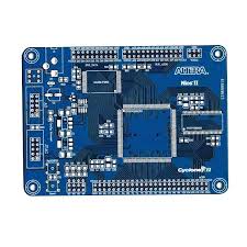
1. High-Density Interconnect (HDI) PCBs
How They Work
HDI PCBs are designed to accommodate more components in a smaller space by using microvias, finer traces, and higher layer counts. These boards utilize:
- Laser-drilled microvias (smaller than traditional through-holes)
- Sequential lamination to build multiple layers efficiently
- Thinner dielectric materials to reduce spacing between layers
Benefits
- Increased Circuit Density: More functionality in a compact design.
- Improved Signal Integrity: Shorter trace lengths reduce signal loss.
- Better Thermal Management: Efficient heat dissipation due to optimized layouts.
- Lightweight & Space-Saving: Ideal for smartphones, wearables, and IoT devices.
2. Flexible and Rigid-Flex PCBs
How They Work
- Flexible PCBs: Made from polyimide or other flexible substrates, allowing bending and folding.
- Rigid-Flex PCBs: Combine rigid and flexible sections for structural stability and dynamic flexibility.
Benefits
- Durability: Withstand vibrations and mechanical stress.
- Reduced Weight & Space: Eliminate connectors, reducing overall size.
- Design Freedom: Can be shaped to fit unconventional spaces (e.g., medical implants, foldable electronics).
- Improved Reliability: Fewer solder joints mean fewer failure points.
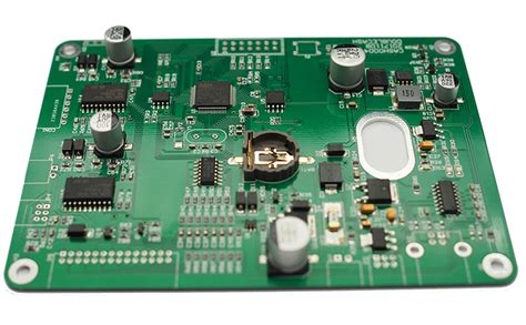
3. Embedded Components
How They Work
Instead of mounting components on the surface, they are embedded within the PCB layers using:
- Passive components (resistors, capacitors) printed into the substrate.
- Active components (ICs) placed in cavities and laminated over.
Benefits
- Space Efficiency: Frees up surface area for other components.
- Enhanced Performance: Reduced parasitic inductance/capacitance for high-speed circuits.
- Improved Durability: Protects components from environmental damage.
- Better Thermal Management: Heat is distributed more evenly.
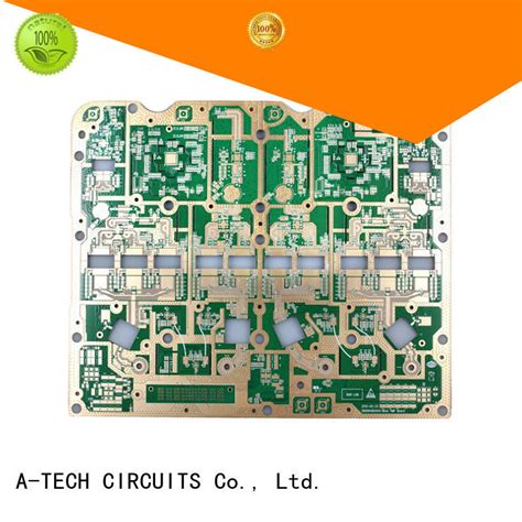
4. Advanced PCB Materials
How They Work
Traditional FR-4 is being replaced by high-performance materials like:
- Rogers, Teflon, and Ceramic-filled laminates for high-frequency applications.
- Thermally conductive substrates for better heat dissipation.
- Low-loss dielectrics for high-speed digital circuits.
Benefits
- Higher Signal Speeds: Essential for 5G, RF, and millimeter-wave applications.
- Improved Thermal Stability: Reduces warping and delamination.
- Longer Lifespan: Resists moisture, chemicals, and extreme temperatures.
5. High-Frequency PCBs
How They Work
Designed for RF, microwave, and high-speed digital signals, these PCBs use:
- Specialized substrates (PTFE, hydrocarbon ceramics).
- Controlled impedance traces to minimize signal loss.
- EMI shielding techniques to reduce interference.
Benefits
- Minimal Signal Loss: Critical for radar, satellite, and telecom systems.
- Reduced Crosstalk: Tight impedance control ensures signal clarity.
- Better Heat Resistance: Handles high-power RF applications.
6. Advanced Manufacturing Techniques
How They Work
- 3D Printing (Additive Manufacturing): Allows rapid prototyping of complex PCB geometries.
- Automated Optical Inspection (AOI): Ensures precision and reduces defects.
- Semi-Additive Processes (SAP): Enables ultra-fine traces (< 10µm).
Benefits
- Faster Turnaround: Accelerates product development.
- Higher Precision: Reduces manufacturing errors.
- Cost-Effective for Prototyping: Ideal for R&D and small batches.
Conclusion
Advanced PCB options are revolutionizing electronics by enabling smaller, faster, and more reliable devices. From HDI and flexible PCBs to embedded components and high-frequency materials, these innovations cater to the demands of modern technology, including 5G, AI, IoT, and aerospace applications.
By leveraging these advanced techniques, manufacturers can achieve:
✔ Higher performance in compact designs.
✔ Improved durability in harsh environments.
✔ Greater design flexibility for next-gen electronics.
As PCB technology continues to evolve, we can expect even more breakthroughs that push the boundaries of what’s possible in electronics.