How are multilayer pcbs made
Materials And Components Used In Multilayer PCB Manufacturing
Multilayer printed circuit boards (PCBs) are integral to modern electronics, providing the necessary infrastructure for complex circuitry in a compact form. The manufacturing of these sophisticated boards involves a variety of materials and components, each playing a crucial role in ensuring the final product’s functionality and reliability. Understanding the materials and components used in multilayer PCB manufacturing is essential for appreciating the intricacies of this advanced technology.
To begin with, the base material, or substrate, is fundamental to the construction of multilayer PCBs.
Typically, this substrate is made from fiberglass-reinforced epoxy resin, known as FR4. FR4 is favored for its excellent mechanical strength, thermal stability, and electrical insulation properties. The substrate serves as the foundation upon which the entire PCB structure is built, providing the necessary support for the conductive layers and components.
Next, the conductive layers, usually made of copper, are critical for forming the electrical pathways on the PCB.
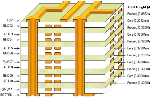
Copper is chosen for its superior electrical conductivity and ease of etching, which allows for precise patterning of the circuit traces. These copper layers are laminated onto the substrate using a combination of heat and pressure, ensuring a strong bond that can withstand the rigors of electronic operation. The number of copper layers can vary, with multilayer PCBs typically containing anywhere from four to over twenty layers, depending on the complexity of the design.
In addition to the substrate and copper layers, the dielectric material is another essential component in multilayer PCB manufacturing.
Dielectric materials, such as prepreg (pre-impregnated composite fibers), are used to separate the conductive layers and provide electrical insulation. Prepreg consists of fiberglass cloth impregnated with resin, which, when heated and pressed, cures to form a solid insulating layer. This dielectric layer not only insulates the conductive layers but also contributes to the overall mechanical stability of the PCB.
Furthermore, the vias, or vertical interconnect accesses, are crucial for establishing electrical connections between the different layers of a multilayer PCB.
Vias are small holes drilled through the PCB, which are then plated with copper to create conductive pathways. There are various types of vias, including through-hole vias, blind vias, and buried vias, each serving specific purposes in the design and functionality of the PCB. Through-hole vias extend through the entire board, while blind vias connect outer layers to inner layers without passing through the entire board, and buried vias connect inner layers without reaching the outer surfaces.
Additionally, solder mask and silkscreen are important components in the manufacturing process.
The solder mask is a protective layer applied over the copper traces to prevent short circuits and corrosion, while also aiding in the soldering process by keeping solder confined to the designated pads. The silkscreen layer, on the other hand, is used to print labels, component identifiers, and other markings on the PCB, facilitating assembly and troubleshooting.
Moreover, the choice of components to be mounted on the PCB, such as resistors, capacitors, integrated circuits, and connectors, is critical to the board’s functionality. These components are selected based on the specific requirements of the electronic device and are mounted using surface-mount technology (SMT) or through-hole technology (THT), depending on the design and application.
In conclusion, the materials and components used in multilayer PCB manufacturing are diverse and meticulously chosen to ensure the performance and reliability of the final product. From the substrate and conductive layers to the dielectric materials, vias, solder mask, silkscreen, and mounted components, each element plays a vital role in the intricate process of creating multilayer PCBs. Understanding these materials and components provides valuable insight into the complexity and precision involved in modern electronics manufacturing.

Step-By-Step Process Of Multilayer PCB Fabrication
The fabrication of multilayer printed circuit boards (PCBs) is a complex and meticulous process that involves several critical steps to ensure the final product meets the required specifications and performance standards. Initially, the process begins with the design phase, where engineers use specialized software to create a detailed blueprint of the PCB layout. This design includes the arrangement of various layers, the placement of components, and the routing of electrical connections. Once the design is finalized, it is converted into a format suitable for manufacturing, typically Gerber files.
Following the design phase, the next step is the preparation of the substrate material, usually a fiberglass-reinforced epoxy laminate known as FR4.
This material serves as the foundation for the PCB. The substrate is cleaned thoroughly to remove any contaminants that could affect the adhesion of subsequent layers. After cleaning, a thin layer of copper is laminated onto both sides of the substrate. This copper layer will form the basis for the conductive pathways on the PCB.
The process then moves to the creation of the inner layers.
Each inner layer is printed with a photoresist, a light-sensitive material that hardens when exposed to ultraviolet (UV) light. The photoresist is applied to the copper-clad substrate, and a photomask, which contains the desired circuit pattern, is placed over it. The assembly is then exposed to UV light, which hardens the photoresist in the areas not covered by the photomask. The unhardened photoresist is subsequently washed away, revealing the copper underneath. The exposed copper is then etched away using a chemical solution, leaving behind the desired circuit pattern. This process is repeated for each inner layer of the PCB.
Once all the inner layers are created, they are carefully aligned and laminated together under high pressure and temperature.
This lamination process fuses the layers into a single, solid board. After lamination, the outer layers of the PCB are processed in a similar manner to the inner layers. A photoresist is applied, exposed to UV light through a photomask, and developed to reveal the circuit pattern. The exposed copper is etched away, leaving the desired circuitry on the outer layers.
Following the creation of the outer layers, the next step is drilling.
Precision drilling machines create holes for vias, which are used to connect different layers of the PCB, as well as holes for mounting components. These holes are then plated with copper to ensure electrical connectivity between layers. The entire board is then coated with a layer of solder mask, which insulates the copper traces and prevents short circuits. The solder mask is applied as a liquid and then cured under UV light.
The final steps in the fabrication process include the application of a silkscreen layer, which adds labels and markings to the PCB, and the application of a surface finish, such as HASL (Hot Air Solder Leveling) or ENIG (Electroless Nickel Immersion Gold), to protect the exposed copper and ensure good solderability. The completed PCB undergoes rigorous testing, including electrical tests to verify connectivity and functionality, as well as visual inspections to check for any defects.
In conclusion, the fabrication of multilayer PCBs involves a series of precise and carefully controlled steps, from design and material preparation to layer creation, lamination, drilling, and finishing. Each step is crucial to ensuring the final product meets the stringent requirements of modern electronic devices.
Contact us for PCB quote now |
Challenges And Solutions In Multilayer PCB Production
The production of multilayer printed circuit boards (PCBs) presents a unique set of challenges that require innovative solutions to ensure high-quality and reliable end products. One of the primary challenges in multilayer PCB production is the precise alignment of the multiple layers. Each layer must be accurately aligned to ensure that the electrical connections between them are correct. Misalignment can lead to short circuits, open circuits, or other functional failures. To address this, manufacturers employ advanced alignment techniques, such as optical alignment systems, which use cameras and software to ensure that each layer is perfectly positioned before lamination.
Another significant challenge is the lamination process itself.
Multilayer PCBs are created by stacking several layers of conductive and insulating materials, which are then bonded together under heat and pressure. This process must be carefully controlled to prevent defects such as delamination, where layers separate, or voids, which are air pockets trapped between layers. To mitigate these issues, manufacturers use high-quality materials and precise temperature and pressure controls. Additionally, vacuum lamination techniques can be employed to remove air and ensure a more uniform bond between layers.
Thermal management is also a critical concern in multilayer PCB production.
As electronic devices become more powerful and compact, the heat generated by components can increase significantly. Effective thermal management is essential to prevent overheating and ensure the longevity and reliability of the PCB. Manufacturers address this challenge by incorporating thermal vias, which are small holes filled with conductive material that help dissipate heat. Additionally, advanced materials with better thermal conductivity, such as metal-core PCBs, can be used to enhance heat dissipation.
The complexity of the electrical connections in multilayer PCBs also poses a challenge.
With multiple layers, the routing of electrical traces becomes more intricate, increasing the risk of signal interference and crosstalk. To overcome this, manufacturers use advanced design software that can simulate the electrical performance of the PCB and optimize the layout to minimize interference. Additionally, techniques such as differential pair routing and controlled impedance can be employed to ensure signal integrity.
Quality control is another critical aspect of multilayer PCB production.
Given the complexity and precision required, thorough testing is essential to identify and rectify any defects. Manufacturers use a variety of testing methods, including automated optical inspection (AOI), X-ray inspection, and electrical testing, to ensure that each PCB meets the required specifications. AOI uses cameras to inspect the PCB for visual defects, while X-ray inspection can reveal hidden issues such as internal voids or misaligned layers. Electrical testing verifies that the PCB functions correctly by checking for continuity and proper electrical performance.
In conclusion, the production of multilayer PCBs involves addressing several challenges, including precise layer alignment, effective lamination, thermal management, complex electrical routing, and rigorous quality control. By employing advanced technologies and techniques, manufacturers can overcome these challenges and produce high-quality, reliable multilayer PCBs that meet the demands of modern electronic devices. The continuous evolution of materials, design software, and manufacturing processes will further enhance the capabilities and performance of multilayer PCBs, ensuring their continued relevance in the ever-advancing field of electronics.
Contact us for PCB quote now |
Quality Control And Testing In Multilayer PCB Manufacturing
Quality control and testing are critical components in the manufacturing of multilayer printed circuit boards (PCBs). These processes ensure that the final product meets the stringent requirements of performance, reliability, and durability. The complexity of multilayer PCBs, which can consist of multiple layers of conductive material separated by insulating layers, necessitates rigorous testing at various stages of production to identify and rectify any potential issues.
Initially, the raw materials used in the production of multilayer PCBs undergo thorough inspection.
This includes checking the quality of the copper-clad laminates, prepreg materials, and other essential components. Ensuring the purity and consistency of these materials is vital, as any defects can compromise the integrity of the final product. Once the materials pass the initial inspection, the manufacturing process begins with the creation of individual layers.
During the layer formation stage, each layer is meticulously inspected for defects such as scratches, pinholes, or contamination. Automated optical inspection (AOI) systems are commonly employed to detect these imperfections. AOI systems use high-resolution cameras and advanced algorithms to compare the produced layers against the original design files, identifying any discrepancies that could affect the PCB’s performance.
After the individual layers are verified, they are laminated together under high pressure and temperature to form a single, cohesive unit. This lamination process is critical, as any misalignment or air entrapment between layers can lead to electrical failures. Post-lamination, the multilayer PCB undergoes another round of inspection to ensure that the layers are correctly aligned and free from defects.
Electrical testing is another crucial aspect of quality control in multilayer PCB manufacturing.
This involves checking for continuity and isolation between the various conductive paths. Flying probe testers and bed-of-nails testers are commonly used for this purpose. These testing methods help identify open circuits, short circuits, and other electrical anomalies that could impair the functionality of the PCB.
In addition to electrical testing, thermal stress testing is performed to evaluate the PCB’s ability to withstand extreme temperatures. This is particularly important for PCBs used in high-reliability applications such as aerospace, automotive, and medical devices. Thermal cycling tests expose the PCB to repeated cycles of high and low temperatures, simulating real-world operating conditions. Any delamination, cracking, or other thermal-induced failures are identified and addressed during this phase.
Furthermore, solderability testing is conducted to ensure that the PCB’s surface finish is compatible with the soldering process.
Poor solderability can lead to weak joints and unreliable connections, which can compromise the overall performance of the PCB. This testing involves dipping the PCB into molten solder and evaluating the wetting properties of the surface finish.
Finally, a visual inspection is carried out to check for any cosmetic defects such as discoloration, warping, or surface irregularities. While these defects may not necessarily impact the electrical performance of the PCB, they can affect the overall quality and reliability of the product.
In conclusion, quality control and testing are indispensable in the manufacturing of multilayer PCBs. From the initial inspection of raw materials to the final visual check, each step is meticulously designed to ensure that the PCB meets the highest standards of quality and reliability. By employing a combination of automated and manual inspection techniques, manufacturers can identify and rectify potential issues early in the production process, thereby delivering a product that performs reliably in its intended application.
YouTube URL
Paste a link to the content you want to display on your site.Embed
Contact us for PCB quote now |
Interlinks Options
Toggle panel: Interlinks Options
WPCode Page Scripts
Toggle panel: WPCode Page ScriptsPostBlock
How are multilayer pcbs made
Set featured imageAdd an excerpt…
2,251 words, 12 minutes read time.
Last edited 28 minutes ago.
StatusDraft
PublishImmediately
Link/how-are-multilayer-pcbs-made
AuthorGrace
TemplateDefault template
DiscussionOpen
Step-By-Step Process Of Multilayer PCB Fabrication
The fabrication of multilayer printed circuit boards (PCBs) is a complex and meticulous process that involves several critical steps to ensure the final product meets the required specifications and performance standards. Initially, the process begins with the design phase, where engineers use specialized software to create a detailed blueprint of the PCB layout. This design includes the arrangement of various layers, the placement of components, and the routing of electrical connections. Once the design is finalized, it is converted into a format suitable for manufacturing, typically Gerber files.
Following the design phase, the next step is the preparation of the substrate material, usually a fiberglass-reinforced epoxy laminate known as FR4.
This material serves as the foundation for the PCB. The substrate is cleaned thoroughly to remove any contaminants that could affect the adhesion of subsequent layers. After cleaning, a thin layer of copper is laminated onto both sides of the substrate. This copper layer will form the basis for the conductive pathways on the PCB.
The process then moves to the creation of the inner layers.
Each inner layer is printed with a photoresist, a light-sensitive material that hardens when exposed to ultraviolet (UV) light. The photoresist is applied to the copper-clad substrate, and a photomask, which contains the desired circuit pattern, is placed over it. The assembly is then exposed to UV light, which hardens the photoresist in the areas not covered by the photomask. The unhardened photoresist is subsequently washed away, revealing the copper underneath. The exposed copper is then etched away using a chemical solution, leaving behind the desired circuit pattern. This process is repeated for each inner layer of the PCB.
Once all the inner layers are created, they are carefully aligned and laminated together under high pressure and temperature.
This lamination process fuses the layers into a single, solid board. After lamination, the outer layers of the PCB are processed in a similar manner to the inner layers. A photoresist is applied, exposed to UV light through a photomask, and developed to reveal the circuit pattern. The exposed copper is etched away, leaving the desired circuitry on the outer layers.
Following the creation of the outer layers, the next step is drilling.
Precision drilling machines create holes for vias, which are used to connect different layers of the PCB, as well as holes for mounting components. These holes are then plated with copper to ensure electrical connectivity between layers. The entire board is then coated with a layer of solder mask, which insulates the copper traces and prevents short circuits. The solder mask is applied as a liquid and then cured under UV light.
The final steps in the fabrication process include the application of a silkscreen layer, which adds labels and markings to the PCB, and the application of a surface finish, such as HASL (Hot Air Solder Leveling) or ENIG (Electroless Nickel Immersion Gold), to protect the exposed copper and ensure good solderability. The completed PCB undergoes rigorous testing, including electrical tests to verify connectivity and functionality, as well as visual inspections to check for any defects.
In conclusion, the fabrication of multilayer PCBs involves a series of precise and carefully controlled steps, from design and material preparation to layer creation, lamination, drilling, and finishing. Each step is crucial to ensuring the final product meets the stringent requirements of modern electronic devices.
Challenges And Solutions In Multilayer PCB Production
The production of multilayer printed circuit boards (PCBs) presents a unique set of challenges that require innovative solutions to ensure high-quality and reliable end products. One of the primary challenges in multilayer PCB production is the precise alignment of the multiple layers. Each layer must be accurately aligned to ensure that the electrical connections between them are correct. Misalignment can lead to short circuits, open circuits, or other functional failures. To address this, manufacturers employ advanced alignment techniques, such as optical alignment systems, which use cameras and software to ensure that each layer is perfectly positioned before lamination.
Another significant challenge is the lamination process itself.
Multilayer PCBs are created by stacking several layers of conductive and insulating materials, which are then bonded together under heat and pressure. This process must be carefully controlled to prevent defects such as delamination, where layers separate, or voids, which are air pockets trapped between layers. To mitigate these issues, manufacturers use high-quality materials and precise temperature and pressure controls. Additionally, vacuum lamination techniques can be employed to remove air and ensure a more uniform bond between layers.
Thermal management is also a critical concern in multilayer PCB production.
As electronic devices become more powerful and compact, the heat generated by components can increase significantly. Effective thermal management is essential to prevent overheating and ensure the longevity and reliability of the PCB. Manufacturers address this challenge by incorporating thermal vias, which are small holes filled with conductive material that help dissipate heat. Additionally, advanced materials with better thermal conductivity, such as metal-core PCBs, can be used to enhance heat dissipation.
The complexity of the electrical connections in multilayer PCBs also poses a challenge.
With multiple layers, the routing of electrical traces becomes more intricate, increasing the risk of signal interference and crosstalk. To overcome this, manufacturers use advanced design software that can simulate the electrical performance of the PCB and optimize the layout to minimize interference. Additionally, techniques such as differential pair routing and controlled impedance can be employed to ensure signal integrity.
Quality control is another critical aspect of multilayer PCB production.
Given the complexity and precision required, thorough testing is essential to identify and rectify any defects. Manufacturers use a variety of testing methods, including automated optical inspection (AOI), X-ray inspection, and electrical testing, to ensure that each PCB meets the required specifications. AOI uses cameras to inspect the PCB for visual defects, while X-ray inspection can reveal hidden issues such as internal voids or misaligned layers. Electrical testing verifies that the PCB functions correctly by checking for continuity and proper electrical performance.
In conclusion, the production of multilayer PCBs involves addressing several challenges, including precise layer alignment, effective lamination, thermal management, complex electrical routing, and rigorous quality control. By employing advanced technologies and techniques, manufacturers can overcome these challenges and produce high-quality, reliable multilayer PCBs that meet the demands of modern electronic devices. The continuous evolution of materials, design software, and manufacturing processes will further enhance the capabilities and performance of multilayer PCBs, ensuring their continued relevance in the ever-advancing field of electronics.
Quality Control And Testing In Multilayer PCB Manufacturing
Quality control and testing are critical components in the manufacturing of multilayer printed circuit boards (PCBs). These processes ensure that the final product meets the stringent requirements of performance, reliability, and durability. The complexity of multilayer PCBs, which can consist of multiple layers of conductive material separated by insulating layers, necessitates rigorous testing at various stages of production to identify and rectify any potential issues.
Initially, the raw materials used in the production of multilayer PCBs undergo thorough inspection.
This includes checking the quality of the copper-clad laminates, prepreg materials, and other essential components. Ensuring the purity and consistency of these materials is vital, as any defects can compromise the integrity of the final product. Once the materials pass the initial inspection, the manufacturing process begins with the creation of individual layers.
During the layer formation stage, each layer is meticulously inspected for defects such as scratches, pinholes, or contamination. Automated optical inspection (AOI) systems are commonly employed to detect these imperfections. AOI systems use high-resolution cameras and advanced algorithms to compare the produced layers against the original design files, identifying any discrepancies that could affect the PCB’s performance.
After the individual layers are verified, they are laminated together under high pressure and temperature to form a single, cohesive unit. This lamination process is critical, as any misalignment or air entrapment between layers can lead to electrical failures. Post-lamination, the multilayer PCB undergoes another round of inspection to ensure that the layers are correctly aligned and free from defects.
Electrical testing is another crucial aspect of quality control in multilayer PCB manufacturing.
This involves checking for continuity and isolation between the various conductive paths. Flying probe testers and bed-of-nails testers are commonly used for this purpose. These testing methods help identify open circuits, short circuits, and other electrical anomalies that could impair the functionality of the PCB.
In addition to electrical testing, thermal stress testing is performed to evaluate the PCB’s ability to withstand extreme temperatures. This is particularly important for PCBs used in high-reliability applications such as aerospace, automotive, and medical devices. Thermal cycling tests expose the PCB to repeated cycles of high and low temperatures, simulating real-world operating conditions. Any delamination, cracking, or other thermal-induced failures are identified and addressed during this phase.
Furthermore, solderability testing is conducted to ensure that the PCB’s surface finish is compatible with the soldering process.
Poor solderability can lead to weak joints and unreliable connections, which can compromise the overall performance of the PCB. This testing involves dipping the PCB into molten solder and evaluating the wetting properties of the surface finish.
Finally, a visual inspection is carried out to check for any cosmetic defects such as discoloration, warping, or surface irregularities. While these defects may not necessarily impact the electrical performance of the PCB, they can affect the overall quality and reliability of the product.
In conclusion, quality control and testing are indispensable in the manufacturing of multilayer PCBs. From the initial inspection of raw materials to the final visual check, each step is meticulously designed to ensure that the PCB meets the highest standards of quality and reliability. By employing a combination of automated and manual inspection techniques, manufacturers can identify and rectify potential issues early in the production process, thereby delivering a product that performs reliably in its intended application.