How Are Those Dense Vias on PCBs Arranged?
Introduction
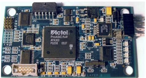
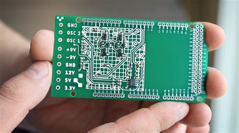
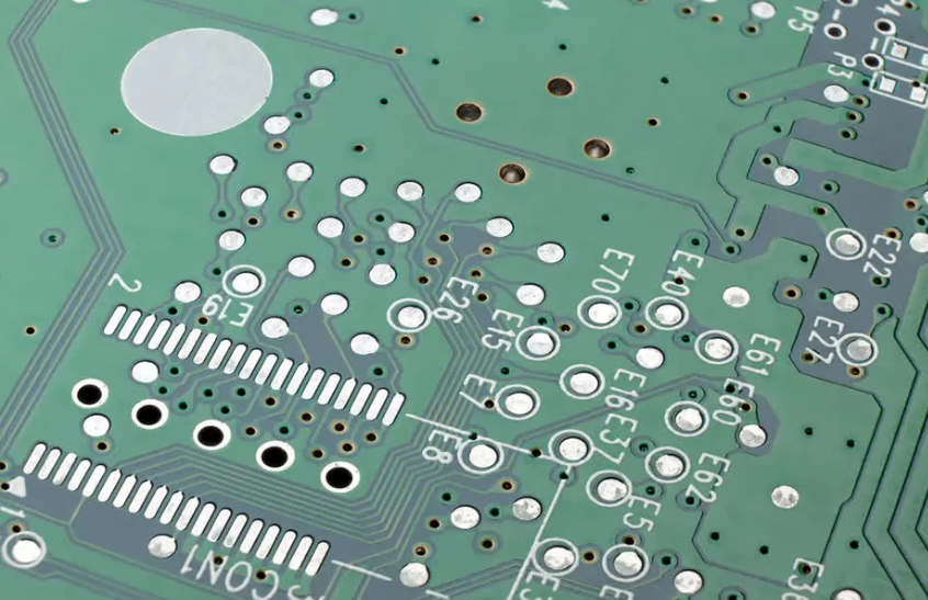
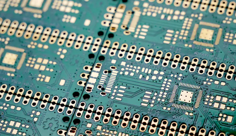
Printed Circuit Boards (PCBs) are the backbone of modern electronics, and one of their most distinctive features is the presence of numerous small holes called vias. These vias serve as vertical interconnection access points, allowing electrical connections between different layers of a multi-layer PCB. As electronic devices have become more compact and complex, the density of vias on PCBs has increased dramatically. This article explores the fascinating world of via arrangement in high-density PCB designs, examining the principles, techniques, and considerations that govern their placement.
Understanding PCB Vias
Before delving into arrangement patterns, it’s essential to understand what vias are and their various types:
- Through-hole vias: Span the entire thickness of the PCB
- Blind vias: Connect an outer layer to one or more inner layers but don’t go through the entire board
- Buried vias: Connect inner layers without reaching either surface
- Microvias: Extremely small vias (typically less than 150 microns in diameter) often used in high-density designs
Each type serves specific purposes in PCB design and affects how vias can be arranged on the board.
Factors Influencing Via Arrangement
Several critical factors determine how vias are arranged on a PCB:
1. Electrical Requirements
The primary function of vias is to provide electrical connectivity between layers. The arrangement must ensure:
- Proper signal integrity
- Minimal impedance mismatches
- Adequate current-carrying capacity
- Controlled impedance for high-speed signals
2. Thermal Considerations
Vias play a crucial role in thermal management:
- Heat dissipation from components
- Thermal relief connections
- Prevention of thermal stress concentration
3. Manufacturing Constraints
PCB fabrication capabilities limit via arrangements:
- Minimum via diameter and pitch
- Aspect ratio limitations (depth to diameter ratio)
- Registration tolerances between layers
- Plating quality requirements
4. Mechanical Factors
The physical arrangement affects board reliability:
- Structural integrity of the PCB
- Resistance to mechanical stress
- Prevention of via cracking under thermal cycling
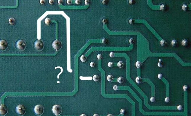
Common Via Arrangement Patterns
PCB designers employ several systematic approaches to arrange dense vias:
1. Grid-Based Arrangements
The most fundamental approach uses regular geometric patterns:
Rectangular Grid
- Vias placed at regular intervals in orthogonal directions
- Simple to implement and route
- Efficient for many digital circuits
Hexagonal Grid
- Vias arranged in a honeycomb pattern
- Provides more uniform distribution
- Can offer better signal integrity in some cases
2. Functional Groupings
Vias are clustered based on circuit functionality:
Component-Centric Arrangement
- Vias grouped around specific components
- Follows component pinouts
- Common for BGA and other high-pin-count packages
Signal-Type Grouping
- Power vias clustered together
- Ground vias arranged in specific patterns
- Signal vias grouped by frequency or function
3. Escape Routing Patterns
For high-density components like BGAs, vias are arranged to “escape” signals from the component:
Staggered Patterns
- Alternate rows offset to increase routing channels
- Allows more traces between via rows
- Common in fine-pitch BGA designs
Via-in-Pad
- Vias placed directly in component pads
- Maximizes space utilization
- Requires careful manufacturing control
Advanced Via Arrangement Techniques
As PCB densities increase, designers employ more sophisticated techniques:
1. High-Density Interconnect (HDI) Strategies
HDI designs use microvias and specialized arrangements:
Stacked Vias
- Multiple microvias stacked vertically
- Enables connections through many layers
- Requires precise alignment
Staggered Vias
- Offset microvias between layers
- Reduces stress concentration
- Easier to manufacture than stacked vias
2. Differential Pair Via Arrangement
For high-speed differential signals:
- Symmetrical placement of paired vias
- Maintained consistent spacing
- Often includes ground vias for shielding
3. Power Delivery Network (PDN) Via Arrays
Optimized arrangements for power distribution:
- Dense via arrays under power pins
- Strategic placement to minimize voltage drop
- Often follows component power requirements
Design Tools and Automation
Modern PCB design relies heavily on software tools for via arrangement:
1. Autorouters with Via Management
Advanced autorouting algorithms that:
- Automatically place vias during routing
- Optimize via placement for density and performance
- Enforce design rule constraints
2. Constraint-Driven Design
Design environments where via placement follows:
- Electrical constraints (impedance, crosstalk)
- Thermal requirements
- Manufacturing rules
3. Design Rule Checking (DRC)
Automated verification that ensures:
- Proper via spacing
- Adequate clearance
- Manufacturability compliance
Manufacturing Considerations
The arrangement of dense vias must account for production realities:
1. Drilling Limitations
Mechanical drilling has practical limits:
- Minimum hole size (typically 0.15mm for mechanical drills)
- Maximum aspect ratio (usually 10:1 or less)
- Board thickness constraints
2. Laser Drilling for Microvias
Enables smaller vias but with its own constraints:
- Limited depth capability
- Tapered via profiles
- Higher cost compared to mechanical drilling
3. Plating Challenges
High-density via arrangements affect:
- Plating uniformity
- Via fill quality
- Reliability of the final product
Future Trends in Via Arrangement
The evolution of PCB technology continues to push via density:
1. Smaller Via Sizes
Ongoing reductions in via diameters:
- Microvias below 50 microns
- Laser and material advancements enabling smaller features
2. 3D Arrangement Optimization
Advanced modeling for:
- Thermal performance optimization
- Signal integrity analysis
- Mechanical stress minimization
3. Alternative Via Technologies
Emerging approaches like:
- Conductive ink vias
- Photonic interconnects
- Wireless vertical connections
Conclusion
The arrangement of dense vias on modern PCBs represents a complex interplay of electrical, thermal, mechanical, and manufacturing considerations. From simple grid patterns to sophisticated 3D arrangements, via placement has evolved into a precise science that balances competing requirements. As electronic devices continue to shrink while increasing in capability, the art and science of via arrangement will remain a critical aspect of PCB design, pushing the boundaries of what’s possible in electronics packaging and interconnection.
Understanding these principles not only helps in appreciating the complexity behind modern electronics but also underscores the remarkable engineering achievements that enable the devices we use every day. The seemingly random scattering of tiny holes on a PCB is, in fact, a carefully orchestrated pattern that embodies both technical necessity and engineering elegance.