How Are Vias Developed in Embedded PCB Design?
Introduction to PCB Vias in Embedded Systems
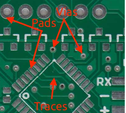
Printed Circuit Boards (PCBs) form the backbone of all modern embedded systems, providing the physical platform for electrical connections between components. Among the most critical elements in PCB design are vias – the conductive pathways that connect different layers of a multilayer board. In embedded system development, where space constraints, signal integrity, and thermal management are paramount, via design becomes particularly crucial.
Vias serve as vertical interconnect access points, allowing signals and power to travel between the various layers of a PCB. Their proper implementation can mean the difference between a reliable, high-performance embedded system and one plagued with signal integrity issues, thermal problems, or manufacturing defects. This article explores the comprehensive process of via development in embedded PCB design, covering types, design considerations, manufacturing processes, and advanced techniques.
Types of Vias in Embedded PCB Design
Through-Hole Vias
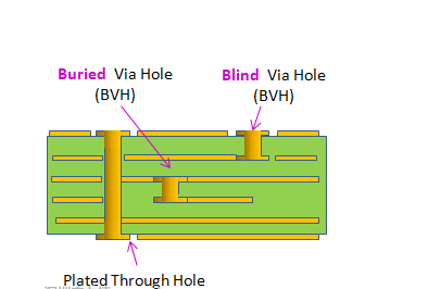
The most common and traditional type, through-hole vias span the entire thickness of the PCB. These vias are drilled through all layers and then plated to create electrical connectivity between layers. In embedded systems, through-hole vias are often used for:
- Connecting power and ground planes
- Providing structural support for components
- Creating thermal pathways for heat dissipation
- High-reliability applications where robustness is critical
While through-hole vias offer excellent reliability, they consume significant board space and can create obstacles for high-density routing in compact embedded designs.
Blind Vias
Blind vias connect an outer layer of the PCB to one or more inner layers but do not pass through the entire board. These are particularly valuable in embedded systems where:
- High component density requires efficient use of board space
- Signal integrity must be maintained by minimizing stub lengths
- Layer count is high (8+ layers), making full through-vias impractical
The fabrication of blind vias is more complex than through-hole vias, often requiring sequential lamination processes or laser drilling techniques.
Buried Vias
Buried vias exist entirely within the inner layers of the PCB, connecting two or more internal layers without reaching either outer surface. Embedded system designers utilize buried vias to:
- Maximize routing density on surface layers
- Reduce the number of through-vias that could obstruct routing channels
- Maintain signal integrity by providing more direct interlayer connections
The manufacturing process for buried vias is the most complex among standard via types, typically requiring multiple lamination steps during PCB fabrication.
Microvias
Defined as vias with a diameter of 150 microns (6 mils) or less, microvias have become essential in modern embedded system design, particularly for:
- High-density interconnect (HDI) PCBs
- Fine-pitch ball grid array (BGA) component breakout
- High-speed digital circuits requiring minimized via stub effects
Microvias are almost exclusively created using laser drilling technology due to the precision required. They can be stacked or staggered to create connections through multiple layers in HDI designs.
Design Considerations for Vias in Embedded Systems
Electrical Considerations
Signal Integrity: Via design significantly impacts signal integrity in high-speed embedded systems. Key factors include:
- Impedance matching through careful via geometry control
- Minimizing via stub lengths, especially for high-frequency signals
- Proper placement relative to transmission lines to reduce reflections
Current Carrying Capacity: Vias must be sized appropriately for their current load:
- Power and ground vias typically require larger diameters
- Multiple parallel vias may be needed for high-current paths
- Thermal considerations affect current capacity ratings
Thermal Management
Embedded systems often face thermal challenges, and vias play a crucial role:
- Thermal vias conduct heat away from hot components to inner layers or heat sinks
- Via patterns under high-power components help distribute thermal loads
- Airflow considerations may affect via placement in convection-cooled systems
Manufacturing Constraints
Design for Manufacturing (DFM) principles guide via design:
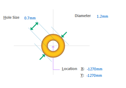
- Minimum via sizes based on fabrication capabilities
- Aspect ratio limitations (typically 8:1 or 10:1 for reliable plating)
- Clearance requirements from other features
- Registration tolerances for multilayer alignment
The Via Development Process in Embedded PCB Design
1. Schematic Capture and Netlist Generation
The via development process begins during schematic capture, where the electrical connections between components are defined. While specific via locations aren’t determined at this stage, the connectivity requirements that will drive via placement are established.
2. Component Placement and Floorplanning
As components are placed on the PCB layout, the need for interlayer connections becomes apparent. Critical considerations include:
- Identifying escape routing paths from high-pin-count components
- Planning power distribution network (PDN) via placement
- Anticipating high-speed signal routing requirements
3. Routing Strategy Development
The PCB designer develops a routing strategy that accounts for:
- Layer stackup configuration
- Signal class segregation (digital, analog, RF, power)
- Impedance control requirements
- Crosstalk mitigation approaches
This strategy directly influences via placement and selection of via types.
4. Via Placement and Optimization
Actual via placement involves:
- Selecting appropriate via types for each connection
- Determining optimal via locations to minimize signal path lengths
- Balancing via density with manufacturability
- Implementing via stitching for shielding or thermal purposes
Advanced EDA tools often include via optimization features that can:
- Automatically replace through-vias with blind/buried vias where possible
- Suggest via locations to minimize layer transitions
- Optimize via patterns for high-speed signals
5. Design Rule Checking (DRC)
Comprehensive DRC verifies that all vias comply with:
- Fabrication capabilities (minimum hole size, annular ring)
- Electrical requirements (clearances, current capacity)
- Assembly constraints (solder mask clearance)
- Reliability standards (aspect ratios, plating requirements)
6. Signal Integrity Analysis
For critical signals, additional analysis ensures via performance:
- 3D electromagnetic simulation of critical via structures
- Time-domain reflectometry (TDR) analysis for impedance matching
- Crosstalk evaluation between adjacent vias
Manufacturing Processes for PCB Vias
Drilling Technologies
Mechanical Drilling:
- Used for standard through-hole vias (>150μm diameter)
- High-speed CNC machines with carbide drill bits
- Typical minimum hole size around 100-150μm (4-6 mils)
Laser Drilling:
- Essential for microvias (<150μm diameter)
- Two main types: UV lasers (excimer) and CO₂ lasers
- Can create blind vias with precise depth control
- Enables higher density interconnects
Plating Processes
Electroless Copper Deposition:
- Initial conductive layer applied to via walls
- Provides base for subsequent electroplating
- Ensures uniform coverage throughout via barrel
Electrolytic Copper Plating:
- Builds up copper thickness in vias and on surfaces
- Critical for achieving desired current carrying capacity
- Must maintain uniform thickness in high aspect ratio vias
Via Filling and Capping
Conductive Via Filling:
- Used for thermal vias or to create flat surfaces for component mounting
- Typically filled with conductive epoxy or electroplated copper
- Improves thermal conductivity and reliability
Non-Conductive Via Filling:
- Prevents solder wicking during assembly
- Provides planar surface for fine-pitch components
- Often uses epoxy-based materials
Via Capping:
- Additional copper plating over filled vias
- Creates smooth, flat surface for component mounting
- Essential for via-in-pad applications
Advanced Via Technologies for Embedded Systems
High-Density Interconnect (HDI) Via Structures
Stacked Microvias:
- Microvias aligned vertically through multiple layers
- Provides most compact vertical interconnection
- Requires precise alignment control during lamination
Staggered Microvias:
- Offset microvias connected by short traces
- Reduces stress concentration compared to stacked vias
- Slightly less dense but often more reliable
Via-in-Pad Technology
Direct component termination to vias:
- Eliminates need for fanout traces
- Maximizes space utilization in dense designs
- Requires careful via filling and planarization
Embedded Component Technology
Components mounted within PCB layers:
- Utilizes specialized via structures for interconnection
- Enables ultra-compact embedded system designs
- Requires advanced manufacturing techniques
Reliability Considerations for Embedded System Vias
Thermal Cycling Reliability
Embedded systems often operate in environments with temperature fluctuations:
- Different CTE (Coefficient of Thermal Expansion) between copper and PCB material causes stress
- Via barrel cracks can develop over many thermal cycles
- Proper via design minimizes stress concentrations
Mechanical Stress Resistance
Vias must withstand:
- Board flexing in portable embedded devices
- Vibration in automotive or industrial applications
- Mechanical shock from drops or impacts
Electromigration Concerns
High-current vias risk:
- Metal ion migration under high current density
- Progressive resistance increase over time
- Potential open circuit failure
Future Trends in Via Technology for Embedded Systems
3D Printed Electronics
Emerging additive manufacturing techniques enable:
- Novel via structures impossible with traditional methods
- Graded material properties within vias
- Integrated component-via structures
Advanced Materials
New substrate materials require via technology adaptation:
- High-frequency laminates with specialized plating requirements
- Flexible circuits with stretchable via interconnects
- Thermally conductive substrates for improved heat dissipation
Photonic Interconnects
Potential future development:
- Optical vias for board-level photonic connections
- Hybrid electrical/optical interconnection
- Enabling next-generation high-bandwidth embedded systems
Conclusion
The development of vias in embedded PCB design represents a critical intersection of electrical engineering, materials science, and manufacturing technology. As embedded systems continue to push the boundaries of miniaturization, performance, and functionality, via technology must evolve correspondingly. From basic through-hole vias to sophisticated HDI microvia structures, the proper implementation of vias remains fundamental to successful embedded system design.
Designers must balance electrical requirements, thermal considerations, mechanical reliability, and manufacturing constraints when developing via strategies for embedded PCBs. With the ongoing trends toward higher density, higher frequency, and more compact embedded solutions, via technology will continue to be an area of intense innovation in the electronics industry.
The comprehensive understanding of via development processes enables embedded system designers to create more reliable, higher performance products while meeting the ever-increasing demands of modern electronic applications. As we look to the future, advancements in via technology will play a pivotal role in enabling the next generation of embedded computing solutions.


