How Impedance Is Used in PCB Layout Importance of Impedance vs. Resistance in PCB Layout
When designing a circuit board layout, it can be easy to identify a routine where certain parameters are given more importance than others. This is even more common when the parameters are interdependent or vary with each other. For example, resistance is actually or can be used to represent all other electrical parameters in a circuit. Yet, this important parameter is not usually considered when laying out a PCB. On the other hand, impedance derived from resistance is a common design factor.
Let’s explore this question by looking at how impedance is used to create a circuit board layout and how resistance affects the design process. This will allow us to compare impedance vs. resistance to determine which is more important for laying out a PCB.
How Impedance is Used in PCB Layout
The PCB layout design process can be roughly divided into the following activities:
- Major PCB layout tasks
- Material selection tasks
- Select layer materials
- Define layer thickness
- Select solder mask type
- Layout tasks
- Determine component placement locations
- Determine drill and via placement
- Routing tasks
- Set trace copper weight
- Set trace length and width
- Define trace path
- Via type definition
- Design checks
- DFM compatibility
- PDN analysis
- Thermal analysis
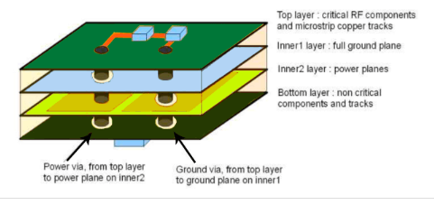
Of the major layout tasks listed above, the material selection and routing tasks are most dependent on impedance parameters. For example, it is common practice to define a fixed impedance, which in turn defines a dielectric constant, which is used to define and select the type of material used for layer stackup, as shown below.
Fixed Impedance Stackup
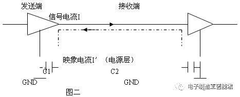
For trace routing, impedance is also a major factor. This is especially true for high-speed RF signals, as changes in impedance can cause signal integrity issues. Such as noise. Therefore, impedance is indeed important for PCB layout design, but what about resistance?
The Effect of Resistance on PCB Layout
In some cases, impedance can be analyzed without including resistors or real elements. For example, when reactance is much larger and resistance is negligible. However, in reality, resistance plays a role in all circuits because it affects current levels. For PCB design, transmission lines or traces are relatively short, and copper, which has the lowest resistivity, is the most commonly used material. Therefore, actual power losses are usually not an issue. However, eddy currents or I2R losses due to changes in magnetic fields are an issue.
For board layout design, resistance is often considered when performing design checks; such as power distribution (PDN) and/or thermal analysis. These analyses are usually done by simulating the operation of the board under desired input and environmental conditions (similar to the nominal conditions of an assembled PCB or PCBA deployment). In contrast to PDN simulation, the main goal of thermal analysis is to determine how heat is distributed along the surface and throughout the board. This is important in determining what heat dissipation and/or distribution techniques and equipment are needed to ensure the manufacturability and operation of the board. Thermal analysis and PDN can be performed separately (e.g., through different software tools) or using a single high-level tool; such as Cadence’s Celsius Solver.
The importance of resistance in power distribution and thermal analysis is based on the fact that changes in heat can significantly change the properties of materials; such as resistance. Now, we know that both impedance and resistance are important for PCB layout design. But is one more important than the other?
Impedance vs. impedance or impedance vs. resistance for board layout?
As mentioned above, it is not a question of whether impedance or resistance is important for PCB layout design. Clearly, both are important, as shown in the table below.
The table indicates which major PCB layout tasks depend primarily on impedance and/or resistance. From this perspective, neither of these parameters can be said to be more important than the other. Therefore, for a good PCB layout design, you should take advantage of both where they have an impact.