How multilayer pcb are made
Understanding The Basics Of Multilayer PCB Design
Multilayer printed circuit boards (PCBs) are a cornerstone of modern electronics, enabling the compact and efficient design of complex electronic devices. Understanding the basics of multilayer PCB design involves delving into the intricacies of their structure, fabrication, and the advantages they offer over simpler designs.
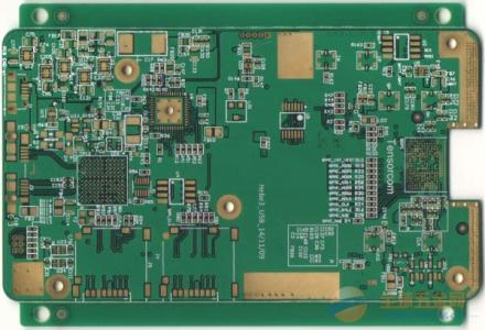
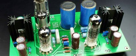
At the heart of a multilayer PCB is its layered construction, which typically consists of three or more conductive layers.
These layers are separated by insulating materials known as substrates, often made from fiberglass or other composite materials. The conductive layers are usually made of copper and are etched with intricate patterns to form the necessary electrical circuits.
The design process begins with a schematic, which is a detailed diagram of the electronic circuit.
This schematic is translated into a layout that specifies the placement of components and the routing of electrical connections across the various layers. Advanced software tools are employed to optimize this layout, ensuring that the design meets electrical performance criteria while minimizing the physical size of the board. Once the design is finalized, the fabrication process can commence.
This involves several key steps, starting with the creation of individual layers.
Each layer is produced by laminating a thin sheet of copper onto a substrate, followed by the application of a photosensitive film. The desired circuit pattern is then transferred onto the film using ultraviolet light, a process known as photolithography. The exposed areas of copper are etched away, leaving behind the intricate circuit patterns.
Subsequently, these individual layers are aligned and bonded together under heat and pressure to form a single, cohesive unit.
This lamination process is critical, as it ensures the mechanical stability and electrical integrity of the multilayer PCB. Through-holes, or vias, are then drilled into the board to establish electrical connections between the layers. These vias are plated with copper to ensure reliable conductivity. The final steps in the fabrication process include the application of a solder mask, which protects the copper traces from oxidation and prevents solder bridges during component assembly. A silkscreen layer is also added to provide labels and markings for component placement. The board is then subjected to rigorous testing to verify its electrical performance and structural integrity.
The advantages of multilayer PCBs are manifold. They offer increased circuit density, allowing for more complex designs within a smaller footprint.
This is particularly beneficial in applications where space is at a premium, such as in smartphones and other portable devices. Additionally, multilayer PCBs can provide improved electrical performance, as the close proximity of the layers reduces the length of electrical paths and minimizes signal interference. This is crucial in high-speed and high-frequency applications, where signal integrity is paramount.
In conclusion, the design and fabrication of multilayer PCBs are intricate processes that require careful planning and precision. By understanding the basics of multilayer PCB design, one can appreciate the technological advancements that have made modern electronics possible. The ability to pack more functionality into smaller spaces without compromising performance is a testament to the ingenuity and innovation inherent in multilayer PCB technology. As electronic devices continue to evolve, the role of multilayer PCBs will undoubtedly remain pivotal in shaping the future of electronics.
Step-By-Step Guide To Multilayer PCB Fabrication
The fabrication of multilayer printed circuit boards (PCBs) is a complex process that requires precision and expertise. This intricate procedure begins with the design phase, where engineers use specialized software to create a detailed blueprint of the PCB. The design includes the layout of the circuitry, the placement of components, and the number of layers required. Once the design is finalized, it is converted into a format suitable for manufacturing, typically a Gerber file, which serves as a digital map for the fabrication process.
Following the design phase, the next step is the preparation of the raw materials.
The core of a multilayer PCB is typically made from a fiberglass-reinforced epoxy laminate, known as FR-4. This material provides the necessary structural support and insulation. Copper foil is then laminated onto both sides of the core material. The number of copper layers depends on the complexity of the PCB, with more layers allowing for more intricate circuitry.
The process continues with the creation of the inner layers. Each layer is printed with a photoresist, a light-sensitive material that hardens when exposed to ultraviolet light.
The Gerber files guide the exposure process, ensuring that only the desired areas of the photoresist are hardened. The unhardened photoresist is then removed, revealing the copper beneath. This exposed copper is etched away using a chemical solution, leaving behind the desired circuit pattern.
Once the inner layers are completed, they are aligned and laminated together under high pressure and temperature.
This step is crucial, as any misalignment can lead to a malfunctioning PCB. The layers are bonded with a resin, which hardens to form a solid structure. After lamination, the outer layers are added, following the same process of applying photoresist, exposure, and etching.
Drilling is the next critical step in the fabrication process.
Precision drilling machines create holes for vias, which are small conductive pathways that connect different layers of the PCB. These holes are then plated with copper to ensure electrical connectivity. The plating process involves immersing the board in a copper solution and applying an electric current, which deposits a thin layer of copper onto the walls of the holes.
Subsequently, the PCB undergoes a solder mask application.
The solder mask is a protective layer that prevents solder from bridging between conductive traces, thereby reducing the risk of short circuits. It also provides a surface for the application of silkscreen, which is used to print labels and component identifiers on the board.
Finally, the PCB is subjected to electrical testing to verify its functionality.
This involves checking for continuity and ensuring that there are no short circuits or open circuits. Any defects identified during testing are addressed before the PCB is approved for assembly.
In conclusion, the fabrication of multilayer PCBs is a meticulous process that involves several stages, each requiring careful attention to detail. From design to testing, each step is crucial in ensuring the final product meets the required specifications and functions as intended. This comprehensive approach to PCB fabrication underscores the importance of precision and expertise in the production of these essential components in modern electronics.
Materials And Techniques Used In Multilayer PCB Manufacturing
In the realm of modern electronics, multilayer printed circuit boards (PCBs) have become indispensable due to their ability to support complex circuitry in a compact form. The manufacturing of these sophisticated components involves a meticulous process that combines advanced materials and techniques to ensure functionality and reliability. Understanding the materials and techniques used in multilayer PCB manufacturing provides insight into the intricate nature of these essential electronic components.
To begin with, the foundation of any multilayer PCB is the substrate material, typically composed of fiberglass-reinforced epoxy resin, known as FR-4
This material is favored for its excellent insulating properties, mechanical strength, and thermal stability, making it ideal for supporting the multiple layers of conductive pathways. The choice of substrate is crucial, as it must withstand the thermal and mechanical stresses encountered during both the manufacturing process and the operational life of the PCB.
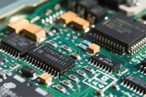
Once the substrate is prepared, the next step involves the application of copper layers, which serve as the conductive pathways for electrical signals.
These copper layers are laminated onto the substrate using a combination of heat and pressure, ensuring a strong bond. The number of copper layers can vary depending on the complexity of the circuit design, with some multilayer PCBs containing upwards of 20 layers. Each layer is separated by a dielectric material, which acts as an insulator to prevent electrical interference between adjacent layers.
The process of creating the intricate circuit patterns on each copper layer is achieved through a technique known as photolithography.
This involves coating the copper surface with a light-sensitive photoresist material, which is then exposed to ultraviolet light through a mask that outlines the desired circuit pattern. The exposed areas of the photoresist harden, while the unexposed areas remain soft and are subsequently removed, revealing the underlying copper. The exposed copper is then etched away using a chemical solution, leaving behind the precise circuit pattern.
Following the etching process, the individual layers are aligned and laminated together under high pressure and temperature to form a single, cohesive unit.
This lamination process is critical, as it ensures the structural integrity and electrical performance of the multilayer PCB. The alignment of the layers must be precise to avoid any misalignment that could lead to circuit failure.
Once laminated, the multilayer PCB undergoes a series of drilling operations to create vias, which are small holes that allow electrical connections between the different layers.
These vias are then plated with copper to ensure conductivity. The final steps in the manufacturing process include the application of a solder mask, which protects the copper traces from oxidation and prevents solder bridges during component assembly, and the application of a silkscreen layer, which provides labels and markings for component placement.
In conclusion, the manufacturing of multilayer PCBs is a complex process that requires a careful selection of materials and precise execution of techniques. From the choice of substrate and copper layers to the intricate processes of photolithography and lamination, each step is critical in producing a reliable and efficient multilayer PCB. As technology continues to advance, the demand for these sophisticated components will only increase, underscoring the importance of understanding the materials and techniques involved in their production.
Quality Control And Testing In Multilayer PCB Production
In the intricate world of electronics manufacturing, the production of multilayer printed circuit boards (PCBs) stands as a testament to technological advancement and precision engineering. As these complex components form the backbone of modern electronic devices, ensuring their quality and reliability is paramount. The process of quality control and testing in multilayer PCB production is a meticulous endeavor, designed to guarantee that each board meets stringent industry standards and performs flawlessly in its intended application.
To begin with, the journey of quality assurance in multilayer PCB production starts at the design phase.
Engineers employ advanced software tools to simulate and validate the design, ensuring that it adheres to the required specifications and performance criteria. This initial step is crucial, as any oversight at this stage can lead to costly errors later in the production process. Once the design is finalized, it is translated into a series of manufacturing instructions that guide the fabrication of the PCB.
As the production process commences, raw materials undergo rigorous inspection to verify their compliance with quality standards
. The substrates, copper foils, and other essential materials are scrutinized for defects, such as impurities or inconsistencies, which could compromise the integrity of the final product. This careful selection of materials sets the foundation for a high-quality multilayer PCB.
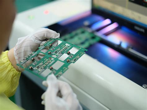
During the fabrication phase, each layer of the PCB is meticulously constructed and aligned.
The process involves etching, laminating, and drilling, all of which require precision and accuracy. To ensure that these steps are executed flawlessly, manufacturers employ automated equipment and advanced imaging technologies. These tools not only enhance the precision of the manufacturing process but also facilitate real-time monitoring, allowing for immediate detection and correction of any deviations from the desired specifications.
As the multilayer PCB takes shape, it undergoes a series of intermediate inspections.
Optical inspection systems are employed to examine the alignment and registration of each layer, while automated optical inspection (AOI) machines scan for defects such as shorts, opens, or misalignments. These inspections are critical in identifying potential issues early in the production process, thereby minimizing the risk of defects in the final product.
Once the PCB is fully assembled, it is subjected to a battery of tests to verify its functionality and reliability.
Electrical testing, including continuity and isolation tests, is conducted to ensure that the circuit paths are correctly formed and that there are no unintended connections. Additionally, more advanced testing methods, such as flying probe testing and in-circuit testing, are employed to assess the performance of the PCB under simulated operating conditions.
Environmental testing is another crucial aspect of quality control in multilayer PCB production.
These tests expose the PCB to various environmental stresses, such as temperature fluctuations, humidity, and vibration, to evaluate its durability and resilience. By simulating real-world conditions, manufacturers can ensure that the PCB will perform reliably throughout its intended lifespan.
In conclusion, the quality control and testing processes in multilayer PCB production are comprehensive and multifaceted, encompassing every stage from design to final inspection. Through meticulous attention to detail and the use of advanced technologies, manufacturers are able to produce PCBs that meet the highest standards of quality and reliability. This commitment to excellence not only ensures the performance of individual components but also upholds the integrity of the electronic devices that rely on them.