How to Choose the Right PCB Stackup for Your Design
Introduction
Printed Circuit Board (PCB) stackup is one of the most critical design considerations that directly impacts the performance, manufacturability, and reliability of electronic devices. The stackup refers to the arrangement of copper and insulating layers that make up a PCB. Selecting an appropriate stackup is essential for signal integrity, power integrity, electromagnetic compatibility (EMC), thermal management, and mechanical stability.
This comprehensive guide explores the key factors to consider when choosing a PCB stackup, common stackup configurations, and best practices for various applications. Whether you’re designing high-speed digital circuits, RF/microwave systems, or mixed-signal boards, understanding stackup selection will significantly improve your PCB design outcomes.
Fundamentals of PCB Stackup
What is PCB Stackup?
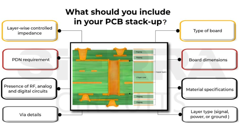
A PCB stackup is the vertical arrangement of conductive copper layers and dielectric insulating materials in a printed circuit board. Modern PCBs typically consist of multiple layers (from 2 to 50+ in complex designs) laminated together under heat and pressure. The stackup defines:
- Number of layers
- Layer types (signal, power, ground)
- Material types and thicknesses
- Copper weights
- Layer sequence and pairing
Why Stackup Matters
The stackup affects nearly every aspect of PCB performance:
- Signal Integrity: Proper layer arrangement minimizes crosstalk and maintains impedance control
- Power Integrity: Effective power distribution networks reduce noise and voltage drops
- EMC/EMI Performance: Good stackup design reduces electromagnetic emissions and susceptibility
- Manufacturing Yield: Appropriate material selection and layer symmetry improve fabrication success
- Cost: Layer count and material choices significantly impact board cost
- Thermal Management: Stackup affects heat dissipation and thermal stress distribution
Key Considerations for Stackup Selection
1. Number of Layers
The first decision in stackup design is determining how many layers your PCB requires. Consider:
- Circuit complexity: More complex designs generally need more layers
- Signal types: High-speed signals often require dedicated layers with proper referencing
- Power requirements: Multiple voltage rails may need separate power planes
- Density: High component density may necessitate additional routing layers
- Cost constraints: Each additional layer increases fabrication cost
Common layer counts:
- 2-layer: Simple, low-cost designs with low component density
- 4-layer: Good balance for many applications (signal-ground-power-signal)
- 6-8 layer: Common for high-speed digital designs
- 10+ layer: Complex systems with multiple high-speed interfaces
2. Layer Arrangement and Sequencing
The order of layers significantly impacts performance:
- Signal layers: Should be adjacent to plane layers for proper return paths
- Power and ground planes: Provide stable references and reduce noise
- Layer pairing: High-speed signals should reference solid planes (not split planes)
General guidelines:
- Place critical signals between ground planes for best shielding
- Avoid adjacent signal layers when possible to prevent crosstalk
- Use symmetrical stackups to prevent warping during manufacturing
- Route high-speed signals on buried layers to reduce EMI
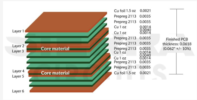
3. Material Selection
PCB materials affect electrical performance, thermal characteristics, and cost:
- FR-4: Standard material for most applications (cost-effective, good mechanical properties)
- High-frequency laminates: (Rogers, Taconic) for RF/microwave applications
- High-Tg materials: For high-temperature environments
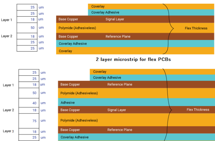
- Flex materials: For rigid-flex designs
Consider:
- Dielectric constant (Dk) and loss tangent (Df) for signal integrity
- Thermal conductivity for heat dissipation
- CTE (Coefficient of Thermal Expansion) matching for reliability
- Moisture absorption characteristics
4. Impedance Control
For high-speed designs, controlled impedance is crucial:
- Determine required impedances (typically 50Ω single-ended, 100Ω differential)
- Calculate trace widths based on dielectric thickness and material properties
- Consider manufacturing tolerances (typically ±10%)
- Use field solvers or impedance calculators for accurate modeling
5. Power Distribution
Effective power delivery requires:
- Dedicated power planes for main voltage rails
- Proper plane capacitance (often with thin dielectrics between power and ground)
- Consideration of DC voltage drop and current capacity
- Decoupling capacitor placement strategy
6. Manufacturability
Ensure your stackup can be reliably fabricated:
- Check with your PCB manufacturer for their capabilities
- Consider minimum dielectric thicknesses
- Account for copper roughness effects at high frequencies
- Maintain symmetry to prevent warpage
- Follow design rules for via structures and layer transitions
Common PCB Stackup Configurations
2-Layer Stackups
Simple and cost-effective but limited in performance:
- Top Layer (Signals/Components)
- Bottom Layer (Signals/Ground)
Best for:
- Low-frequency analog circuits
- Simple digital designs
- Prototyping and hobbyist projects
4-Layer Stackups
The most common configuration for many applications:
- Top Layer (Signals/Components)
- Ground Plane
- Power Plane
- Bottom Layer (Signals)
Alternative:
- Top Layer
- Signal Layer (referenced to Ground)
- Signal Layer (referenced to Power)
- Bottom Layer
Benefits:
- Good signal integrity for moderate speed designs
- Effective power distribution
- Reasonable cost
6-Layer Stackups
Better for high-speed designs:
- Top Layer (Signals)
- Ground Plane
- Signal Layer (High-speed)
- Signal Layer (High-speed)
- Power Plane
- Bottom Layer (Signals)
Alternative:
- Top Layer
- Ground
- Signal
- Ground
- Power
- Bottom Layer
Benefits:
- Excellent signal integrity
- Multiple routing layers
- Good EMI performance
8-Layer and Higher Stackups
For complex, high-performance systems:
Typical 8-layer:
- Top Layer
- Ground
- Signal
- Ground/Power
- Power/Ground
- Signal
- Ground
- Bottom Layer
10+ layer boards allow for:
- Multiple dedicated power planes
- Shielded high-speed channels
- Strict impedance control
- Mixed-signal isolation
Advanced Stackup Considerations
High-Speed Design Stackups
For designs with GHz+ signals:
- Use tightly coupled power-ground plane pairs
- Minimize dielectric thickness between signal and reference planes
- Consider ultra-low-loss materials for critical paths
- Implement back-drilling for via stubs in very high-frequency designs
- Use coplanar waveguide structures where appropriate
Mixed-Signal Stackups
For boards with both analog and digital circuits:
- Separate analog and digital ground planes
- Route analog signals over continuous ground planes
- Place analog circuits in distinct board areas
- Use split power planes or isolated regulators
- Consider ground plane stitching strategies
RF/Microwave Stackups
Special considerations for RF designs:
- Use specialized high-frequency laminates
- Tight control over dielectric thickness
- Careful via transition design
- Often use grounded coplanar waveguide (GCPW) structures
- May require hybrid stackups with multiple materials
HDI (High Density Interconnect) Stackups
For designs with fine pitch components:
- Use microvias and buried vias
- May employ build-up technologies
- Often use very thin dielectrics
- May require sequential lamination processes
- Typically higher layer counts in compact form factors
Practical Stackup Design Process
- Define Requirements:
- Board size constraints
- Signal types and speeds
- Power requirements
- EMC/thermal needs
- Cost targets
- Determine Layer Count:
- Based on routing density
- Signal integrity needs
- Power distribution complexity
- Select Materials:
- Standard FR-4 or specialized materials
- Dielectric thicknesses
- Copper weights
- Create Initial Stackup:
- Assign layer purposes
- Arrange layer sequence
- Calculate impedances
- Validate with Simulations:
- Signal integrity analysis
- Power integrity verification
- Thermal modeling if needed
- Consult with Manufacturer:
- Verify manufacturability
- Adjust based on feedback
- Finalize stackup
- Document Thoroughly:
- Include in fabrication drawings
- Specify all materials and thicknesses
- Note special requirements
Common Stackup Mistakes to Avoid
- Insufficient Ground References:
- Signals without proper return paths
- Split planes under critical traces
- Asymmetric Construction:
- Leading to warpage issues
- Causing impedance variations
- Improper Layer Sequencing:
- Adjacent signal layers causing crosstalk
- High-speed signals far from reference planes
- Ignoring Manufacturing Constraints:
- Unrealistic dielectric thicknesses
- Incompatible material combinations
- Overlooking Thermal Considerations:
- Inadequate heat dissipation
- CTE mismatches in multilayer boards
- Excessive Layer Count:
- Unnecessarily increasing cost
- Adding complexity without benefit
Conclusion
Selecting the optimal PCB stackup is a critical engineering decision that requires balancing multiple technical requirements with cost and manufacturability constraints. By understanding the fundamental principles of stackup design and considering the specific needs of your application, you can create PCBs that deliver reliable performance while meeting all design objectives.
Remember that stackup design is iterative—initial choices may need refinement based on simulations, manufacturer feedback, and prototype testing. Collaborating closely with your PCB fabricator and using modern design tools will help you arrive at the best stackup solution for your particular project.
As technology advances with higher signal speeds, increased integration, and more demanding operating environments, thoughtful stackup design becomes even more essential for successful electronic products. By applying the guidelines presented in this article, engineers can make informed stackup decisions that result in high-performance, manufacturable, and cost-effective PCB designs.