How to Conduct High and Low Temperature Testing for PCB Boards
Introduction
Printed Circuit Boards (PCBs) are essential components in modern electronic devices, and their reliability under extreme temperature conditions is critical for performance and longevity. High and low temperature testing ensures that PCBs can withstand operational stresses in various environments, from freezing cold to scorching heat. This article provides a comprehensive guide on how to perform high and low temperature testing for PCBs, covering test standards, equipment, procedures, and best practices.
1. Understanding High and Low Temperature Testing
High and low temperature testing evaluates a PCB’s ability to function under extreme thermal conditions. The test subjects the board to temperature cycles, simulating real-world scenarios such as:
- High-temperature environments (e.g., automotive engine compartments, industrial machinery).
- Low-temperature environments (e.g., aerospace applications, outdoor electronics in cold climates).
- Thermal shock conditions (sudden temperature changes).
Key Objectives of the Test:
- Identify material expansion/contraction effects.
- Detect solder joint failures.
- Assess component performance under thermal stress.
- Ensure compliance with industry standards (e.g., IPC, MIL-STD, IEC).
2. Test Standards and Specifications
Several industry standards govern PCB thermal testing:
- IPC-9701: Performance test methods for PCB assemblies.
- MIL-STD-810: Environmental engineering considerations for military applications.
- IEC 60068-2-14: Environmental testing for electronic products.
- JEDEC JESD22-A104: Temperature cycling tests for semiconductor devices.
Before testing, determine which standards apply to your PCB based on its intended use.
3. Required Equipment
To conduct high and low temperature testing, you will need:
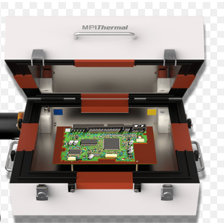
1. Environmental Test Chamber
- A temperature chamber capable of reaching extreme highs (e.g., +125°C) and lows (e.g., -40°C).
- Programmable controllers for automated temperature cycling.
2. Thermal Shock Chamber (Optional for Rapid Cycling Tests)
- Used for sudden temperature transitions (e.g., -55°C to +125°C in seconds).
3. Data Acquisition System
- Monitors temperature, voltage, and resistance changes in real-time.
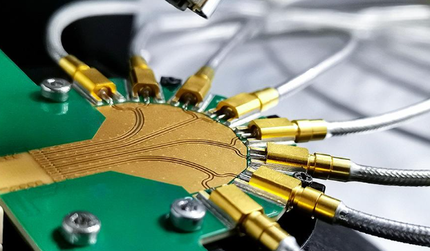
- Thermocouples or infrared sensors for temperature measurement.
4. Test Fixtures and Connectors
- Securely holds the PCB while allowing electrical connections for in-situ testing.
5. Visual Inspection Tools
- Microscopes, magnifiers, or X-ray machines for post-test analysis.
4. Step-by-Step Testing Procedure
Step 1: Pre-Test Preparation
- Review PCB Specifications: Determine the operating temperature range.
- Select Test Parameters: Define temperature extremes, dwell times, and cycle counts.
- Mount the PCB: Secure the board inside the chamber without mechanical stress.
- Connect Monitoring Equipment: Attach thermocouples and data loggers.
Step 2: Initial Visual and Electrical Inspection
- Check for visible defects (cracks, delamination, solder issues).
- Perform baseline electrical tests (continuity, insulation resistance).
Step 3: Temperature Cycling
- Ramp-Up Phase: Gradually increase temperature to the maximum specified limit (e.g., +85°C).
- Dwell Phase: Maintain the high temperature for a set duration (e.g., 30 minutes).
- Ramp-Down Phase: Reduce temperature to the minimum limit (e.g., -40°C).
- Dwell Phase: Hold at low temperature before returning to ambient.
- Repeat Cycles: Conduct multiple cycles (e.g., 50–100) to assess long-term reliability.
Step 4: Intermediate Electrical Testing
- Periodically test functionality during cycles to detect intermittent failures.
Step 5: Post-Test Analysis
- Visual Inspection: Look for cracks, warping, or solder joint failures.
- Electrical Testing: Verify signal integrity, resistance, and insulation.
- Microsectioning (if needed): Examine internal layers for delamination.
5. Common Failure Modes and Analysis
During testing, watch for:
- Solder Joint Cracking: Due to thermal expansion mismatch.
- PCB Warping: Caused by uneven CTE (Coefficient of Thermal Expansion).
- Component Failures: Capacitors, ICs, or connectors may degrade.
- Conductive Anodic Filamentation (CAF): Electrical leakage due to moisture and heat.
6. Best Practices for Accurate Testing
- Use Realistic Temperature Profiles: Match expected field conditions.
- Control Humidity (if applicable): Moisture can accelerate failures.
- Document Every Step: Maintain detailed logs for compliance and troubleshooting.
- Perform Failure Mode Analysis (FMA): Identify root causes of defects.

7. Conclusion
High and low temperature testing is crucial for ensuring PCB reliability in harsh environments. By following standardized procedures, using appropriate equipment, and analyzing failure modes, manufacturers can improve product durability and meet industry requirements. Proper testing reduces field failures, enhances customer satisfaction, and extends the lifespan of electronic devices.
Implementing a robust thermal testing protocol helps engineers design PCBs that perform reliably, whether in Arctic cold or desert heat. By adhering to best practices and leveraging advanced testing tools, companies can deliver high-quality PCBs capable of withstanding extreme thermal challenges.