How to copy boards?
Speaking of copying boards, you may think that there is no technical content, but those who have really copied should have a deep understanding that it is not that simple.
PCB copying has no software and can only be measured and drawn with a caliper, which is slow and has poor accuracy. It is very easy to copy boards with software. Generally, it is more convenient to use Delta’s copying software. You can scan or take a photo of the PCB board first, then load the picture into the software and copy it. After copying, open it with protel99, and after repairing it, you can save it in a protel99 compatible format. The trouble is that it is more troublesome to convert the PCB diagram to the schematic diagram. It requires experience and a certain foundation to complete it well.
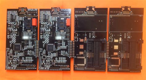
It is more troublesome to copy multi-layer boards because the inner layer cannot be seen and the sample can only be destroyed.
The common method is to copy the top and bottom layers first, and save the photos of the bottom and top layers before removal (for future reference). The accurate method is to remove all components, register all component parameters, and correspond the components to the numbers of the silk screen printing layer one by one. After retaining the original data, take a photo or scan the bare PCB board, and load the obtained photos or scanned images into the software. Different software has different requirements for photo formats. Photo files that are too large will be too large, affecting the copying speed, so oversized PCB boards can be divided into several small pieces for copying, and then spliced. After the upper and lower layers are completed, you can use sandpaper to polish the completed layer on the surface, gradually expose the inner layer, copy one layer, and then grind the next layer until all are completed.
Now there are many well-known copying companies in the industry that can help you complete the copying of those complex PCB boards.
For some relatively simple circuit boards, copying them by yourself is also a very valuable experience. Today, the editor will introduce you to the skills of copying boards.
Required equipment: scanner, computer, PORTEL99 and AUTOCAD software must be installed.
- First put the PCB you want to copy into the scanner, start the scanner, and pay attention to adjust the brightness and contrast in the scanner.
- Open the AUTO CAD software, create a new CAD file, select Insert Dot Image in the Insert menu, and after selecting the image you want to insert, the Insert Image dialog box will appear. Select the ratio of 1:1 in the dialog box.
- After inserting the PCB image, draw a rectangular frame to fit the border of the PCB image. Note that when drawing the border, use the object tracking object lock point. If you don’t draw the border, the image will be accidentally moved during the process of tracing the circuit diagram, and you will have a hard time aligning it.
- Draw component packages. Since the component packages used in the PCB board we want to copy may not match the component packages in PORTEL99, we need to create component packages ourselves, that is, draw the component shapes in the PCB we want to draw. When drawing component packages, we need to count how many types of packages are used on the PCB board. Only one package of each type needs to be drawn. After all the packages are drawn, they need to be transferred to PORTEL 99 for further processing.
- Open PORTEL99, create a new PCB file first, then select Import CAD File in the File menu of PORTEL99 PCB Editor, import the CAD file with the component model drawn, and after the import is successful, the basic graphics of the component package will appear in PORTEL 99 PCB Editor.
- Create a new PCB component editor in PORTEL99, and then open the PCB component editor. After creating a new component, select a component package from the PORTEL99 PCB Editor and copy it to the PCB component editor for component production.
- After all the component packages are made, place them in the PORTEL99 PCB editor and then export them as a CAD file.
- After opening the CAD file of the component package drawing, open the CAD file that previously imported the PCB image, and copy the component package drawing to the CAD with the PCB image. At this time, you can close the CAD file with only the component package drawing. Just work in the CAD file with the PCB image, arrange the components in order according to the component placement angle and position of the PCB image, and pay attention to using the copy and paste method to make more sub-components.
- Place pads and vias: After placing the component package, the next step is to place pads and vias. First, measure the inner and outer diameters of the pads in CAD, then select the ring sub-item in the drawing menu and determine the inner and outer diameters of the ring. When placing pads, pads of the same size should be placed at one time, but square pads and polygonal pads cannot be placed. Although polygons can be filled into entities in CAD, the filled entities will only have an empty border after being transferred to PORTEL 99. Therefore, if there are polygonal pads in the PCB diagram, we can use lines to outline the edges of the pads, and then place the corresponding pads after transferring to PORTEL99.
- Draw the trace: After the pad is drawn, start drawing the trace. The trace is drawn with a polyline. In the drawing menu, select the polyline, determine the starting and ending widths of the polyline, and then start drawing. During the drawing process, if it is a straight line, you must select the orthogonal trace. If it is 45 degrees or other angles, you must cancel the orthogonal trace. If the width of the center line of the entire circuit board has only a few specifications, we can also use ordinary lines to draw, but different line widths must use different layers, and then edit the line width after switching to PORTEL 99.
- After the line drawing is completed, we carry out the last work in CAD, placing the silk screen. If it is text, use the method of placing a text box to achieve it. If it is some irregular silk screen lines, use polylines. Of course, you can also draw directly with lines, and then edit the line width after switching to PORTEL 99.
- After the above steps, the work in CAD has been basically completed. If you do not transfer to PORTEL, you can also let the PCB manufacturer make the board for you. You can also print out the layers you need and make the PCB yourself. Of course, the ultimate purpose of writing this article is to tell readers to transfer the depicted graphics to PORTEL, so we have to continue with the following steps.
- Open the PORTEL99 PCB editor and import the CAD file with the traced lines. Note that in the dialog box of the import file, each layer of CAD should be matched to each layer of PORTEL99. This is very important. No matter what the name of the layer in CAD is, you must know what layer this layer should be in PORTEL99. If you do not control the random import, you will spend more time in PORTEL 99 to convert the layer. In addition, it is best to change the default line width when importing.
- Finally, edit and import PORTEL99, and then make appropriate edits. For example, when we import, we put the circuits and pads on the TOP LAYER layer. At this time, you should put all the pads on the MULTI LAVER layer. Also, no matter what angle you adjust the silkscreen text to in CAD, it will become straight when you transfer it to PORTEL 99. At this time, you need to adjust it according to the actual PCB.
- If there are circuits or silkscreens on the other side, just follow the above method, and then import them into PORTEL 99 for integration. Note that you need to mirror them. Finally, check carefully against the picture or PCB, and you can also make appropriate modifications and you are done.
Notes:
If you accidentally move the picture in CAD, all the lines you draw will be invisible. At this time, you need to move all the pictures away, and then select all the lines you drew.