How to Create the Best PCB Layout for Your Design
Good PCB layout also requires balancing multiple goals. This includes not only following the rules and guidelines for board layout, but also ensuring that your PCB design process encompasses all issues that could impact the manufacturing process and quality of your board. For example, knowing when and how to design for testability (DFT) can significantly impact the turnaround time, quality, and reliability of your design. By defining all of your design goals first, you can strike the right balance. With these, you can come up with the best PCB layout for your design.
What Are PCB Layout Design Goals?
PCB layout design is often viewed as a discrete part of the design phase of board development. It is possible to create a layout in this manner. However, doing so often leads to errors at some point in the development process that may require you to redesign your layout. This unnecessary waste of valuable resources like time and money can be minimized or even eliminated entirely by taking a more holistic view of PCB layout design.
There are specific good practices or tips that should be used for PCB layout design to ensure that your board can be built. However, they should be executed with the overarching goal of achieving the overall goal of your product design intent. These include improving the efficiency of board fabrication and PCB assembly, as well as ensuring that your board meets or exceeds all applicable regulatory requirements and operates reliably throughout its lifecycle.
OBJECTIVE PCB LAYOUT DESIGN
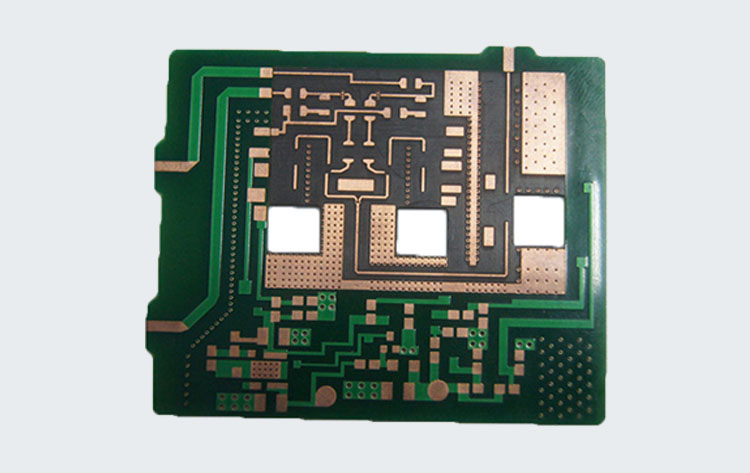
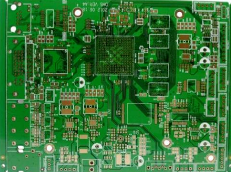
It is indeed the contract manufacturer’s (CM’s) job to build your board according to design specifications. However, it is the designer’s responsibility to ensure that your design files include all information relevant to the fabrication and assembly of your board. This information must contain PCB layout values and tolerances for trace widths, copper weight or thickness, board clearances and drill holes that are customized to your CM’s capabilities; otherwise, you’ll experience delays in clarification and possible redesigns. In addition, you need to make the right choices for your board’s product stackup, including selecting the best materials, choosing the best via options, including the right number of layers and balancing their placement based on the board type. The construction of your board depends on your focus on design for manufacturing (DFM) guidelines based on your CM’s equipment capabilities and processes.
SUPPORTING EFFICIENT PCB ASSEMBLY
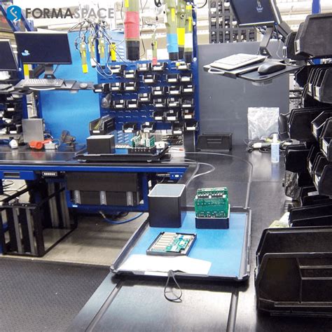
The best DFM guidelines will include some suggestions, tips and requirements to facilitate efficient assembly of your PCB. As. . Knowing the Design for Assembly (DFA) guidelines is meant to enable you to make choices that will not only prevent board assembly stalls, but also help your CM make them. The essential elements of a quality DFA include: ensuring your footprint pads match the components listed in your electronic component list or BOM; using adequate spacing and clearances between board components; selecting adequate solder mask dams and buildouts; utilizing silk screen for markings and identifiers; and applying good thermal dissipation. PCB Assembly (PCBA) starts with having the necessary components for your design. Time spent waiting for ordered components is time lost, and time also adds to your product delivery date. To avoid this, you should optimize your component selection by understanding your component lifecycles and being aware of shortages. Another way you can assist your CM and PCBA is to include a panelization scheme as part of your design. Since boards are often processed in sheets rather than individually, the process includes de-panelization, or breaking the board into sheets. By determining a panelization layout, you eliminate tasks for your CM and can determine which panelization method to use. Designing with this goal in mind will greatly assist your CM and facilitate an efficient PCBA.
Smooth Regulatory Approval
The best designed and manufactured product in the world will never be used unless it can pass all regulatory standards and requirements for the board itself and the components used in it. Depending on the circumstances of your board, there may be many standards that apply for classification, flexibility, and usage. Often, some type of design testing will be necessary, and Design for Testability (DFT) may require steps, including those to prepare the board for testing by the CM. A fundamental goal is to understand what standards apply to your design and how to demonstrate compliance.
Reliable Operation After Deployment
Another consideration that should be addressed throughout the development process is whether the board will be able to perform as designed for its intended lifecycle. Operation and performance are obviously the main drivers behind component selection and schematic creation. However, reaching this goal has broader implications for your PCB layout design, especially the manufacturability of the board and its quality and reliability. The ability of the board to be manufactured as designed depends on the choice of your CM services. For example, should you choose a turnkey service provider or manage multiple companies involved in the different stages of your own manufacturing? If you choose turnkey, you need to consider whether your CM is primarily a manufacturer or an assembler. Subsequently, the quality of the board will depend on your CM’s commitment and approach to implementing quality services. This is even more important if you are developing a critical system. Aerospace, medical device, or automotive industries have strict requirements for quality management. Just as important as the ability of a product to perform its intended function is whether it will do so over its expected operational lifecycle. It would be a mistake to think that board material is the only consideration for reliability. You should also consider how well the board retains its mechanical properties during the manufacturing process. Therefore, you should apply good thermal design principles and don’t neglect the surface finish that your board needs to provide for environmental protection.
Creating the best PCB layout for your design does involve the application of good layout paradigms. However, it should be done from the perspective of meeting the overall design goals. Your CM can be a great asset to you in achieving this goal.