How to design a Multilayer PCB?
When designing a multilayer PCB ,one crucial aspect is planing the multilayer PCB stackup to achieve optimal product performance.A poorly designed substrate and inappropriate material selection can degrade the electrical performance of signal transmission,increase emissions and crosstalk,and make the product more susceptible to external nosie.These issues can lead to intermittent operation,as timing glitches and interference can significantly degrade product performance and long-term reliability.

Multilayer PCB stackup
In contrast,a properly constructed PCB substrate effectively reduces electromagnetic radiation,crosstalk,and improves signal integrity,providing a low-inductance power distribution network.Furthermore,from a manufacturing perspective,this improves product manufacturability.
It makes sense to suppress noise during product production rather than attempting to enhance it.Completing projects”right the first time”on time and on budget means you can reduce costs by shortening design cycles,accelerating time to market,and extending product lifecycles.
Board containing copper planes allow signals routed in a microstrip or stripline controlled impedance transmission line configuration to generate significantly less radiation than indiscriminate traces on a two-layer board.Tightly coupling signals to planes(ground or power)reduces crosstalk and improves signal integrity.
Plane layers in multilayer PCBs significantly reduce radiated emissions over two-layer PCBs.As a rule of thumb,a four-layer board will reduce radiated emissions by 15 dB Compared to a two-sided PCB.
When selecting a multilayer stackup,consider the following factors:
- signal layer should always be adjacent to planes.This limits the number of signal layers embedded bwtween planes to two, and the top and bottom(outer) layer to one signal.
- Signal layer should be tightly coupled(<10mils) to their adjacent planes
- Power planes(as well as ground planes)can be uesd for signal return paths.
- Determine the signal return path(which plane will be used ).Fast rise time signals take the path of least inductance,typically the closest plane.
- Cost(the most important design parameter for bumps)
Solder Mask-Impact on Impedance
Since printed circuit boards are often covered with solder mask,the impact of conformal coating should be considered when calculating Impedance.Typically,solder mask will reduce impedance by 2 to 3 ohms thin traces. As trace thickness increases,the solder mask’s impact becomes less significant.
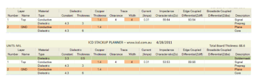
The impact of solder Mask coatings
The figure above illustrates the effect of solder mask coating on microstrip impedance.This example uses a commonly used liquid photoimageable solder mask with a thickness of 0.5 mil and a dielectric constant of 3.3.
The solder mask reduces the microstrip’s characteristic impedance by 2ohms.The differential impedance is 3.5ohms. Therefore,if you don’t account for solder mask,the calculation mat be off by 3% to 4%.
Dielectric Materials
The most popular dielectric material is FR4,which can be either a core material or a prepreg(pre-impregnated)material.The core material is a thin dielectric(cured glass fiber epoxy)with copper foil bonded to both sides.An example is Isola’s FR406 material,which includes 5,8,9.5,14,18,21,28,35,39,47,59,and 93mil cores.Copper thickness typically ranges from ½ to 2 ounces (17 to 70 microns).
Prepreg material is a thin sheet of fiberglass impregnated with uncured expoxy resin that hardens when heated and pressed during the PCB manufacturing process. Isola’s FR406 materials-including 1.7,2.3,3.9,and 7.1MIL prepregs-can be combined to achieve the desired prepreg thickness.
The most common stackup,known as the”foil method”features prepreg with copper foil bonded to the outermost layers(top and bottom),then alternating with prepreg throughout the substrate.Another stackup,known as the “fill method”,is the opposite of the foil method and is used by old-shcool military contractors.
Let’s look at the most common multilayer configurations.
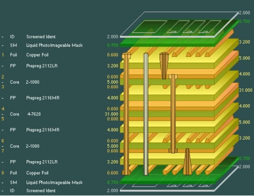
4-layer PCB stackup
A typical four-layer board stackup is shown below.Calculating the substrate’s characteristics and differential impedance.
4-layer PCB stackup
It’s common to see four-layer boards stacked evenly.That is,four evenly spaced layers with the flat surface at the center.While this does make the board symmetrical,it doesn’t help with EMC.
Another common mistake is to tightly couple planes with large dielectric layers and planes between the center and the signal planes.This certainly creates good inter-plane capacitance,but again,it doesn’t help with signal integrity crosstalk,or EMC-which is why we opt for a 4-layer PCB over two layers.
To improve EMC performance on a 4-layer board,it’s best to place signal layer as close to the planes as possible(<10mils) and use a large core(~40mils)between the power and ground planes,keeping the overall substrate thickness to~62mils. Tightly coupling the planed will reduce crosstalk between traces and allow us to keep impedance to an acceptable value.
A good impedance range(Zo)is50 to 60ohms.Keep in mind that lower impedance will increase dI/dt and significantly increase current drawn (bad for a PDN), while higher impedance will emit more EMI and make the design more susceptible to external interference.
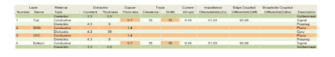
6-Layer PCB stackup
A 6-layer board is essentially a 4-layer board with two additional signal layers added between the planes.This significantly improves EMI by providing two buried layers for high-speed signals and two surface layers for routing low-speed signals.
Signal layers should be placed very close to adjacent planes and require
board thickness(62mil) to consist of a thicker center core.There is always a trade-off between trace impedance,trace width,and prepreg/core thickness,and it’s best to use Rayming’s recommendations for quick”what-if analysis.The Rayming Stackup planner calculates characteristic impedance plus edge-coupled and broadside-coupled differential impedance.The latter applies only to embedded dual stripline layers.Differential pairs are becoming increasingly common in high-speed designs,reducing noise by using differential-mode signaling.

6-layer PCB Stackup
8-layer PCB Stackup
To improve EMC performance ,add two more planes to the six-layer stack up.It is recommended not to have more than two adjacent signal layers between planes,as this creates an impedance between signal layers and increases crosstalk betwwen these signal layers.
In the example below,two plane layers are added to the center of the substrate.This allows for tight coupling between the center planes and isolates each signal plane,reducing coupling that significantly increases crosstalk between these signal layers.
In the example below,two plane layers are added to the center of the substrate.This allows for tight coupling between the center planes and isolates each signal plane,reducing coupling that significantly increases crosstalk. This configuration is commonly used for high-speed signals in DDR2 and DDR3 designs,where crosstalk due to tight routing is a concern.
If you’re risk-averse,this is the right stackup to use.
10-layer PCB Stackup
A ten-layer board should be used when six routing layers and four planes are required,and EMC is a concern.
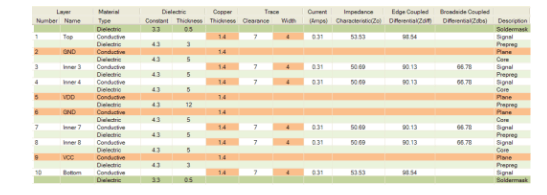
A ten-layer board should be uesd when six routing layers and four planes are required,and EMC is a concern.
10-Layer PCB Stackup
A typical 10-layer stackup is demonstrated above.This stackup is ideal due to the tight coupling of signal and return planes,shielding of high-speed signal layers,the presence of multiple ground planes,and the tightly coupled power/ground plane pair in the center of the board.High-speed signals are typically routed on signal layer buried between planes(in this case,layers 3-4 and7-8).However,care should be taken to route these signals correctly and avoid coupling(crosstalk) between adjacent layers.
12-Layer PCB stackup
12 layers is the maximum number of layers that can typically be conveniently manufactured in a 62ML thick board.Occasionally,you’ll see 14-to 16 layer board fabricated as 62-mil thick board,but the number of manufactures that make them is limited to those capable of producing HDI boards.
High-layer board (over ten) require thin dielectrics(typically 5 mils or less on 62-mil thick board),so they are automatically tightly coupled.
When properly stacked and routed,they can meet all of our high-speed requirements and will have excellent EMC performance and signal integrity.The twelve-layer stackup described above provide shilding on the six inner layers
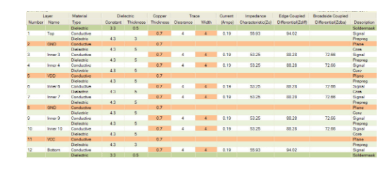
12-Layer PCB stackup
14-layer PCB stackup
The following 14-layer stackup is used when eight routing(signal)layers are required,and special critical shielding is required.Layers 6 and 9 Provide isolation fro sensitive signals,while layers 3 and 4 provide isolation for sensitive signals,While layers 3 and 4 provide
The following 14-layer stackup is used when eight routing (signal) layers are required, and special critical shielding is required. Layers 6 and 9 provide isolation for sensitive signals, while layers 3 and 4 provide shielding for high-speed signals. Layers 11 and 12 provide shielding for high-speed signals.
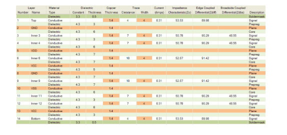
14-Layer PCB Stackup
16-Layer PCB Stackup
16-Layer PCBs offer ten layers of routing and are typically used for extremely dense designs. Often, you’ll see 16-layer PCBs where the routing technology used in EDA applications is unable to route the design to completion. “If it won’t route, just keep adding layers.” While this is a common saying, it’s not a good practice.
If the board won’t route, there could be many reasons. Poor placement is often the course of action. Open routing channels, reduce the number of crossovers in the rat net, place vias on a 25 MIL grid to allow for through routing, and assist the router as much as possible.

16-Layer PCB Stackup
There’s virtually no limit to the number of layers that can be manufactured in a multilayer PCB (please check the manufacturer’s capabilities first). Of course, as the number of layers increases, the board thickness increases to accommodate the minimum thickness of the material used. The aspect ratio (board thickness to minimum aperture) must also be considered. Generally speaking, a 10:1 ratio is recommended for a 100 MIL thick board. For example, a 200-mil thick substrate has a minimum hole size of 20 mil.
Determining the Number of Layers
Technical rules are based on achieving the maximum allowable trace, clearance, and via spacing for the SMT components used, while minimizing PCB manufacturing costs. Complex high-speed designs using ball grid arrays (BGAs) typically require via technology with a 4/4 mil (trace/clearance) and 20/8 mil (pad/hole) spacing. However, lower dimensions can be used if possible; this will reduce costs and improve manufacturing yields.
Once these rules are established, calculate the required characteristic impedance (Zo) and the required differential impedance stackup (Zdiff) based on the component datasheets. Typically, a 50 ohm Zo and a 100 ohm Zdiff are used. Keep in mind that lower impedance increases dI/dt and significantly increases the current drawn (bad for PDNs), while higher impedance generates more EMI and makes the design more susceptible to external interference. Therefore, a good Zo range is 50-60 ohms.
The total number of layers required for a given design depends on its complexity. Factors include: the number of signal nets that must be broken out from the BGA; the amount of power required by the BGA; component density and package type.
Experienced designers will become more accustomed to this over time, but checking for sufficient layers is a good way to automatically adjust the board. If not, the router needs to complete at least 85% of the routing to indicate that the selected stackup is routable. You may need to reevaluate placement several times to achieve optimal results.
How can I calculate the characteristics and differential impedance of the entire stackup using established design rules?
For those unfamiliar with multilayer PCB stackup planning, standard stackups with 2 to 16 layers are provided for common use. However, you can edit, rename, and save your favorite custom stackups for reuse.