How to determine your PCB substrate material
As we all know, the basic properties of PCB (printed circuit board) depend on the performance of its substrate material. Therefore, in order to improve the performance of the circuit board, the performance of the substrate material must be optimized first. So far, various new materials are being developed and applied to meet the requirements that are compatible with new technologies and market trends.
In recent years, the printed circuit board market has undergone a transformation, mainly from traditional hardware products such as desktop computers to wireless communications such as servers and mobile terminals. Mobile communication devices represented by smartphones have promoted the development of PCBs towards high density, lightness and multi-function. Without substrate materials, whose process requirements are closely related to the performance of PCBs, printed circuit technology can never be realized. Therefore, substrate material selection plays a vital role in providing the quality and reliability of PCBs and final products.
Meeting the needs of high density and fine lines
•Requirements for copper foil
All PCB boards are moving towards higher density and finer lines, especially HDI PCBs (high-density interconnect PCBs). Ten years ago, HDI PCBs were defined as PCBs with a line width (L) and line spacing (S) of 0.1mm or less. However, the standard values of L and S in the current electronics industry can be as small as 60μm, and in advanced cases, their values can be as low as 40μm.
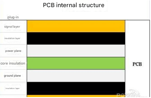
How to determine your PCB substrate material
The traditional method of circuit diagram formation lies in the imaging and etching process, and with the application of thin copper foil substrates (thickness ranging from 9μm to 12μm), the lowest values of L and S reach 30μm.
Due to the high cost of thin copper foil CCL (copper clad laminate) and many defects in stacking, many PCB manufacturers tend to use the etching-copper foil method, and the copper foil thickness is set to 18μm. This method is not actually recommended because it contains too many procedures, the thickness is difficult to control and leads to higher costs. As a result, thin copper foil is better. In addition, when the L and S values of the board are less than 20μm, standard copper foil does not work. Finally, ultra-thin copper foil is recommended because its copper thickness can be adjusted in the range of 3μm to 5μm.
In addition to the thickness of the copper foil, current precision circuits also require a low-roughness copper foil surface. In order to improve the bonding ability of copper foil to substrate material and ensure the peel strength of conductor, rough processing is performed on the copper foil plane, and the ordinary roughness of copper foil is greater than 5μm.
Embedding hump copper foil into the substrate is intended to improve its peel strength. However, in order to control the lead accuracy during circuit etching away from over-etching, it tends to cause hump contaminants, which may cause short circuits between lines or reduced insulation capacity, which especially affects fine circuits. Therefore, copper foil with low roughness (less than 3μm or even 1.5μm) is required.
Despite the reduction of copper foil roughness, it is still necessary to retain the peel strength of the conductor, which causes special surface treatment of the copper foil and substrate material surface, which helps to ensure the peel strength of the conductor.
Requirements for insulating dielectric laminates
One of the main technical characteristics of HDI PCB lies in the construction process. The commonly used RCC (resin coated copper) or prepreg epoxy glass cloth and copper foil lamination rarely leads to fine circuits. Now tend to apply SAP and MSPA, which means applying insulating dielectric film lamination chemical copper plating to produce copper conductive planes. Because the copper plane is thin, fine circuits can be produced.
One of the key points of SAP lies in the lamination dielectric material. In order to meet the requirements of high-density precision circuits, some requirements must be put forward for the lamination materials, including dielectric properties, insulation, heat resistance capacity and bonding, as well as technical adaptability compatible with HDI PCBs.
In global semiconductor packaging, IC packaging substrates are converted from ceramic substrates to organic substrates. The pitch of FC packaging substrates is becoming smaller and smaller, so the current typical values of L and S are 15μm, and it will be smaller.
Multilayer substrate performance should emphasize low dielectricity, low coefficient of thermal expansion (CTE) and high heat resistance, referring to low-cost substrates that meet performance objects. Nowadays, MSPA insulating dielectric lamination technology is combined with thin copper foil and applied to mass production of precision circuits. SAP is used to manufacture circuit patterns with L and S values less than 10μm.
The high density and thinness of PCBs have led to the conversion of HDI PCBs from lamination with cores to any layer cores. For HDI PCBs with the same functions, the area and thickness of interconnected PCBs on any layer are reduced by 25% compared with those with core lamination. A thinner dielectric layer with better electrical performance must be applied in both types of HDI PCBs.
Requirements derived from high frequency and high speed
Electronic communication technology has evolved from wired to wireless, from low frequency and low speed to high frequency and high speed. Smartphone performance has evolved from 4G to 5G, requiring faster transmission speeds and larger transmission volumes.
The advent of the global cloud computing era has led to a multiple increase in data traffic, with an obvious trend of high-frequency and high-speed communication devices. In order to meet the requirements of high-frequency and high-speed transmission, in addition to reducing signal interference and consumption, signal integrity and manufacturing compatible with design requirements in terms of PCB design, high-performance materials are the most important elements.
The main job of engineers is to reduce the properties of electrical signal loss to increase PCB speed, and solve signal integrity issues. Based on PCBCart’s more than ten years of manufacturing services, as a key factor affecting the selection of substrate materials, when the dielectric constant (Dk) is below 4 and the dielectric loss (Df) is below 0.010, it is considered as a medium Dk/Df laminate, and when Dk is below 3.7 and Df is below 0.005, it is considered as a low Dk/Df laminate. At present, a variety of substrate materials can be adopted in the market.
So far, there are three main types of commonly used high-frequency circuit board substrate materials: fluorine-based resins, PPO or PPE resins, and modified epoxy resins. Fluorine-based dielectric substrates, such as PTFE, have the lowest dielectric properties and are generally used for products with a frequency of 5GHz or higher. While modified epoxy resin FR-4 or PPO substrates are suitable for products with a frequency range of 1GHz to 10GHz.
Comparing the three high-frequency substrate materials, epoxy resin has the lowest function price while fluorine-based resin has the highest. In terms of dielectric constant, dielectric loss, water absorption, and frequency characteristics, fluorine-based resins perform best, while epoxy resins perform worse. When the frequency applied to the product is higher than 10GHz, only fluorine-based resins work. The disadvantages of PTFE include high cost, poor rigidity, and high thermal expansion coefficient.
For PTFE, bulk inorganics (such as silica) can be used as filler materials or glass cloth to strengthen the rigidity of the substrate material and reduce the thermal expansion coefficient. In addition, due to the inertness of PTFE molecules, it is difficult for PTFE molecules to bond with copper foil, so special surface treatment compatible with copper foil must be achieved. The treatment method consists in chemical etching on the surface of PTFE to increase the surface roughness or adding an adhesive film to increase the bonding ability. With the application of this method, the dielectric properties may be affected, and further development of the entire fluorine-based high-frequency circuit must be carried out.
Unique insulating resin composed of modified epoxy resin or PPE and TMA, MDI and BMI, plus glass cloth. Similar to FR-4 CCL, it also has excellent heat resistance and dielectric properties, mechanical strength, and manufacturability of PCBs, all of which make it more popular than PTFE-type substrates.
In addition to the performance requirements for insulating materials such as the above-mentioned resins, the surface roughness of copper as a conductor is also an important factor affecting signal transmission loss, which is a result of the skin effect. Basically, the skin effect is that the electromagnetic induction generated on the high-frequency signal transmission and inductance lead becomes so concentrated in the center of the cross-sectional area of the lead that the driving current or signal is focused on the lead surface. The surface roughness of the conductor plays a key role in affecting the transmission signal loss, and low roughness leads to little loss.
At the same frequency, high surface roughness of copper leads to high signal loss. Therefore, the roughness of the surface copper must be controlled in actual manufacturing, and it should be as low as possible without affecting adhesion. Great attention must be paid to signals in the frequency range of 10GHz or higher. The roughness of the copper foil is required to be less than 1μm, and it is best to use an ultra-surface copper foil with a roughness of 0.04μm. The surface roughness of the copper foil must be combined with a suitable oxidation treatment and bonding resin system. In the near future, there may be a copper foil without a profile coating resin, which has a higher peel strength and prevents dielectric loss from being affected.
Requirement for high thermal resistance and high dissipation
With the development trend of miniaturization and high functionality, electronic devices tend to generate more heat, so the thermal management requirements of electronic devices are getting higher and higher demand. One of the solutions to this problem lies in the research and development of thermal conductive PCBs. The basic condition for PCBs to perform well in heat resistance and dissipation is the heat resistance and dissipation capacity of the substrate. The current improvement in the thermal conductivity of PCBs lies in improving through resin and filling addition, but it only works within a limited category. The typical method is to apply IMS or metal core PCBs, which act as heating elements. Compared with traditional heat sinks and fans, this method has the advantages of small size and low cost.
Aluminum is a very attractive material with the advantages of abundant resources, low cost, good thermal conductivity. And strength. In addition, it is so environmentally friendly that it is applied by most metal substrates or metal cores. Due to the advantages of economy, reliable electrical connection, thermal conductivity and high strength, solder-free and lead-free, aluminum-based circuit boards have been applied to consumer products, automobiles, military products and aerospace products. There is no doubt that the heat resistance and dissipation performance of metal substrates, the key lies in the bonding performance between the metal plate and the circuit plane.
How to determine the substrate material of your PCB?
In the modern electronic age, the miniature and thinness of electronic devices have led to the necessary emergence of rigid PCBs and flexible/rigid PCBs. So what type of substrate material is suitable for them?
The increase in the application fields of rigid PCBs and flexible/rigid PCBs has brought new requirements in terms of quantity and performance. For example, polyimide films can be divided into a variety of categories, including transparent, white, black and yellow, with high heat resistance and low thermal expansion coefficient for application in different situations. Similarly, the polyester film substrate with high cost-effectiveness will also be accepted by the market to meet the changing needs of users due to its advantages such as high elasticity, dimensional stability, film surface quality, photoelectric coupling and environmental resistance.
Similar to rigid HDI PCB, flexible PCB must adapt to the requirements of high-speed and high-frequency signal transmission, and attention must be paid to the dielectric constant and dielectric loss of flexible substrate materials. The flexible circuit can be composed of polytetrafluoroethylene and an advancing polyimide substrate. Inorganic dust and carbon fiber can be added to the polyimide resin to result in a three-layer flexible thermal conductive substrate. The inorganic filling material can be aluminum nitride, aluminum oxide or hexagonal boron nitride. This type of substrate material has a thermal conductivity of 1.51W/mK and can resist a voltage of 2.5kV and a curvature of 180 degrees.