How to Distinguish Between Positive and Negative PCB Films: A Comprehensive Guide
Introduction to PCB Films
Printed Circuit Board (PCB) fabrication relies heavily on photographic processes where film plays a critical role in transferring circuit patterns onto copper-clad laminates. Understanding the difference between positive and negative films is fundamental for anyone involved in PCB design, manufacturing, or quality control.
Positive and negative films serve opposite purposes in the PCB manufacturing process, and confusing the two can lead to catastrophic results in board production. This 2000-word guide will provide electronics engineers, PCB designers, and manufacturing technicians with comprehensive knowledge about identifying and working with both types of PCB films.
Fundamental Concepts: Positive vs. Negative Films
Positive Film Characteristics
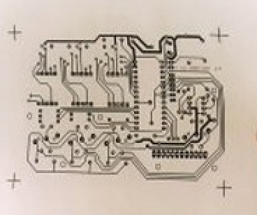
Positive film, sometimes called “positive-working” film, creates a direct correspondence between the film image and the final copper pattern on the PCB:
- Clear areas on the film correspond to areas where copper will be removed during etching
- Dark areas represent copper that will remain on the board
- Produces a positive image of the circuit pattern
- More commonly used in modern PCB manufacturing
- Requires a positive-acting photoresist
When exposed to light through positive film, the exposed areas of positive photoresist become soluble and are washed away during development, leaving the unexposed areas to protect the copper during etching.
Negative Film Characteristics
Negative film creates an inverse relationship between the film image and the final copper pattern:
- Clear areas on the film correspond to copper that will remain on the board
- Dark areas represent areas where copper will be removed
- Produces a negative image of the desired circuit pattern
- More common in older PCB manufacturing processes
- Requires a negative-acting photoresist
With negative film, the exposed areas of negative photoresist become insoluble, while unexposed areas wash away during development. The remaining resist protects copper during etching.
Visual Identification Methods
Side-by-Side Comparison
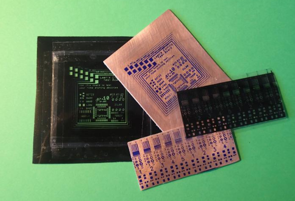
The most straightforward method to distinguish between positive and negative films is to compare them visually:
- Text and Legend Examination:
- On positive film: Text appears normal (readable left-to-right)
- On negative film: Text appears reversed (mirror image)
- Pad and Trace Observation:
- Positive film shows actual pad sizes and trace widths
- Negative film shows inverse spaces between features
- Background Tone:
- Positive film typically has more clear/transparent areas
- Negative film appears darker overall with more opaque areas
Light Table Inspection
Place the film on a light table and examine:
- Positive Film:
- Circuit traces appear black/dark on a clear background
- Similar to how the final PCB copper will look
- Negative Film:
- Clear areas represent where copper will remain
- Background appears dark
- Features look like the “space between” copper traces
Technical Verification Methods
Photoresist Compatibility Test
A small test can determine film type by its interaction with photoresist:
- Apply a small piece of positive-acting photoresist to a test panel
- Expose through a small section of the film
- Develop the resist:
- If exposed areas wash away: Positive film
- If exposed areas remain: Negative film
Dimensional Measurement
Measure specific features on the film and compare to design specifications:
- Positive Film:
- Measured trace widths match design values
- Clearances appear larger than specified
- Negative Film:
- Measured trace widths appear smaller than design
- Clearances match specified values
Manufacturing Process Indicators
Historical Context
Understanding the film’s origin can provide clues:
- Older Processes (pre-2000): More likely to use negative film
- Modern Processes: Predominantly use positive film
- Specific Technologies:
- Additive processes: Typically use negative film
- Subtractive processes: Typically use positive film
Equipment Requirements
The type of photoplotter used can indicate film type:
- Vector Photoplotters: Often produced negative film
- Laser Photoplotters: Typically produce positive film
- Direct Imaging Systems: Usually work with positive data
Common Mistakes and Pitfalls
Incorrect Film Selection Consequences
Using the wrong film type leads to:
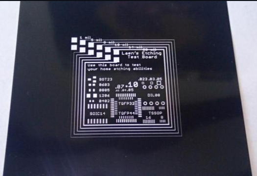
- Complete Circuit Reversal:
- Traces become spaces and spaces become traces
- May create short circuits where opens should be
- May create opens where connections should exist
- Annular Ring Issues:
- Via and through-hole connections may be compromised
- Drilling registration problems
- Solder Mask Problems:
- Mask may cover pads instead of exposing them
- Incorrect mask clearance around features
Verification Best Practices
To avoid costly mistakes:
- Always label films clearly as “POSITIVE” or “NEGATIVE”
- Maintain consistent film type throughout a project
- Verify film type before beginning production
- Implement a two-person verification system for critical boards
Industry Standards and Conventions
IPC Standards Reference
The IPC (Association Connecting Electronics Industries) provides guidelines:
- IPC-2610 series covers PCB documentation requirements
- IPC-4550 series addresses PCB manufacturing processes
- Most contemporary standards assume positive film usage
Common Industry Practices
Modern conventions favor positive film because:
- Design Correspondence: Matches CAD output directly
- Error Reduction: Easier to visually verify
- Process Control: Better for fine-line circuits
- Yield Improvement: Fewer defects in high-density designs
Conversion Between Film Types
Image Reversal Techniques
When necessary, films can be converted:
- Photographic Duplication:
- Copy negative film to create positive
- Copy positive film to create negative
- Requires precision equipment to maintain dimensions
- Digital Conversion:
- Reshoot original artwork with opposite polarity
- Modify Gerber files to reverse image polarity
- Use software like CAM350 or GerberTool for conversion
Considerations for Conversion
Important factors when changing film types:
- Dimensional Stability: Ensure features maintain exact sizes
- Registration Marks: Must remain accurate
- Layer Alignment: Critical for multilayer boards
- Edge Clearance: Verify board outline remains correct
Practical Identification Flowchart
Use this step-by-step approach to determine film type:
- Check for Labeling: Look for “POS” or “NEG” markings
- Inspect Text: Is it readable or mirrored?
- Examine a Known Feature: Compare to design documents
- Evaluate Tone Distribution: More clear or more dark?
- Perform Resist Test: If still uncertain
- Consult Originator: When possible
Future Trends in PCB Imaging
Decline of Traditional Films
The industry is moving toward:
- Direct Imaging (LDI):
- Eliminates film entirely
- Lasers expose resist directly from digital data
- Growing in popularity for high-mix production
- Inkjet PCB Printing:
- Emerging technology
- Deposits etch resist directly
- Potentially disruptive to traditional processes
Implications for Film Identification
As film usage decreases:
- Knowledge Preservation: Still important for legacy products
- Hybrid Systems: Some manufacturers use both methods
- Archive Maintenance: Existing film libraries require management
Conclusion
Accurate identification of positive and negative PCB films remains an essential skill in electronics manufacturing, despite technological advances. By understanding the visual characteristics, technical differences, and manufacturing implications of each film type, professionals can prevent costly errors and ensure proper PCB fabrication.
The key takeaways for distinguishing between positive and negative PCB films are:
- Positive film shows the actual circuit pattern; negative shows its inverse
- Text appears normal on positive film and reversed on negative
- Modern processes predominantly use positive film
- Verification tests can confirm film type when uncertain
- Proper labeling and documentation prevent confusion
As the industry evolves, the fundamental principles of image transfer remain relevant, whether working with traditional films or emerging digital technologies. Mastering these concepts ensures success in PCB manufacturing and maintains quality across all production methods.

