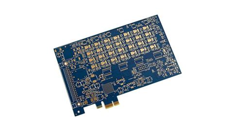
How to Extract PCB Parameters from a DUT (Device Under Test)
Introduction
In modern electronics manufacturing and testing, the ability to extract Printed Circuit Board (PCB) parameters from a Device Under Test (DUT) is crucial for quality control, reverse engineering, and performance validation. This process involves various techniques to measure and analyze electrical, mechanical, and material characteristics of PCBs without damaging the device. This 2000-word article explores the methodologies, tools, and best practices for effectively extracting PCB parameters from DUTs.
Understanding PCB Parameters
Before discussing extraction methods, it’s essential to understand what constitutes PCB parameters:
- Electrical Parameters:
- Trace resistance
- Impedance characteristics
- Capacitance between layers
- Inductance of traces
- Dielectric constant
- Loss tangent
- Physical Parameters:
- Layer thickness
- Trace width and spacing
- Via dimensions
- Copper weight
- Board thickness
- Material Parameters:
- Substrate material composition
- Glass transition temperature (Tg)
- Thermal conductivity
- Coefficient of thermal expansion
- Performance Parameters:
- Signal integrity metrics
- Power integrity characteristics
- Thermal performance
- EMI/EMC characteristics
Non-Destructive Extraction Methods
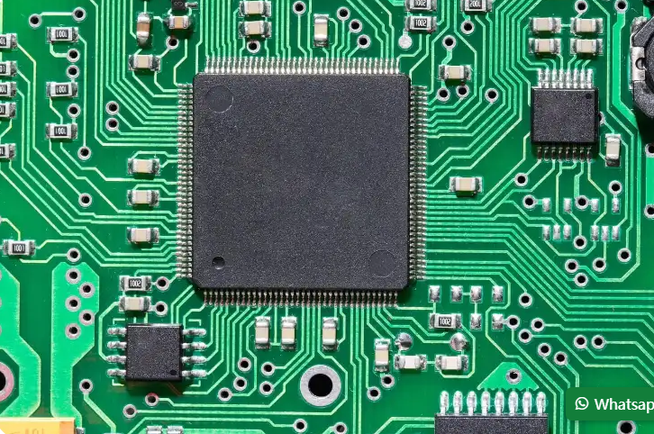
1. Visual Inspection and Optical Measurement
Tools: High-resolution cameras, microscopes, optical comparators
Parameters extracted:
- Trace width and spacing
- Component placement
- Solder joint quality
- Surface defects
Techniques:
- Automated Optical Inspection (AOI)
- 3D optical profilometry
- Image processing algorithms for dimensional analysis
2. X-ray Inspection
Tools: X-ray imaging systems, computed tomography (CT) scanners
Parameters extracted:
- Internal layer structures
- Via and plated through-hole integrity
- Solder joint quality (especially for BGA components)
- Layer alignment (registration)
Advantages:
- Non-destructive internal visualization
- Ability to inspect hidden joints and connections
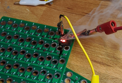
3. Time Domain Reflectometry (TDR)
Tools: High-speed oscilloscopes with TDR modules
Parameters extracted:
- Trace impedance
- Signal propagation delays
- Discontinuities in transmission lines
- Cable and connector quality
Methodology:
- Send a fast electrical pulse through the trace
- Measure reflected signals
- Analyze reflections to determine impedance characteristics
4. Network Analysis
Tools: Vector Network Analyzers (VNA)
Parameters extracted:
- S-parameters (scattering parameters)
- Insertion loss
- Return loss
- Crosstalk between traces
- Frequency-dependent behavior
Approach:
- Measure input and output signals across frequency ranges
- Calculate transfer functions and impedance characteristics
5. Thermal Imaging
Tools: Infrared cameras, thermal sensors
Parameters extracted:
- Temperature distribution
- Hot spots
- Thermal resistance
- Cooling efficiency
Applications:
- Power dissipation analysis
- Thermal management validation
- Identifying short circuits
Destructive Extraction Methods
When non-destructive methods are insufficient, these techniques may be employed:
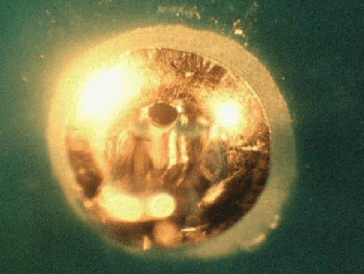
1. Cross-Sectioning
Process:
- Select area of interest
- Cut and polish the PCB to create a clean cross-section
- Examine under microscope
Parameters extracted:
- Layer stack-up verification
- Copper thickness
- Plating quality
- Material interfaces
2. Material Analysis
Techniques:
- Energy Dispersive X-ray Spectroscopy (EDS)
- Fourier Transform Infrared Spectroscopy (FTIR)
- Differential Scanning Calorimetry (DSC)
Parameters extracted:
- Material composition
- Glass transition temperature
- Filler content in substrates
- Contamination analysis
Advanced Techniques for Parameter Extraction
1. Scanning Electron Microscopy (SEM)
Capabilities:
- High-resolution imaging at nanometer scale
- Elemental analysis through EDS
- Topographical information
Applications:
- Fine-pitch trace inspection
- Solder joint analysis
- Failure analysis
2. Terahertz Imaging
Emerging technology for:
- Non-contact thickness measurement
- Delamination detection
- Multi-layer inspection
3. Electrochemical Impedance Spectroscopy (EIS)
Used for:
- Coating quality assessment
- Corrosion analysis
- Conductive material characterization
Software Tools for Parameter Extraction
Modern software plays a crucial role in parameter extraction:
- EDA Tools (e.g., Altium, Cadence):
- Compare measured parameters with design specifications
- Perform signal integrity analysis
- Image Processing Software:
- Automated measurement of physical dimensions
- Defect detection algorithms
- Data Analysis Platforms (e.g., MATLAB, Python libraries):
- Process measurement data
- Create models from extracted parameters
- Perform statistical analysis
Challenges in Parameter Extraction
- Access Limitations:
- Components blocking test points
- Multi-layer boards obscuring internal features
- Measurement Accuracy:
- Calibration requirements
- Environmental factors (temperature, humidity)
- Signal Integrity Issues:
- Probe loading effects
- Ground loop problems
- Data Interpretation:
- Complex interdependencies between parameters
- Frequency-dependent behaviors
Best Practices for Effective Parameter Extraction
- Preparation:
- Review PCB design documents when available
- Identify critical parameters for the specific application
- Plan measurement strategy
- Equipment Selection:
- Choose appropriate tools for target parameters
- Consider measurement resolution requirements
- Verify calibration status
- Measurement Technique:
- Use proper probing techniques
- Minimize interference
- Account for environmental conditions
- Data Management:
- Document measurement conditions
- Store raw data for future reference
- Perform statistical analysis on multiple samples
- Validation:
- Cross-verify with multiple methods when possible
- Compare with design specifications
- Check against known good boards
Case Study: Extracting Impedance Parameters
A practical example of extracting trace impedance:
- Preparation:
- Identify target trace
- Ensure access to both ends
- TDR Measurement:
- Connect TDR to trace via proper probe
- Launch pulse and capture reflection
- Analyze reflection waveform for impedance changes
- VNA Measurement:
- Perform 2-port S-parameter measurement
- Convert S-parameters to impedance values
- Analyze frequency response
- Data Correlation:
- Compare TDR and VNA results
- Resolve discrepancies
- Document final impedance profile
- Design Comparison:
- Compare with expected design values
- Investigate significant deviations
Future Trends in PCB Parameter Extraction
- AI-Assisted Analysis:
- Machine learning for automated defect detection
- Predictive modeling based on extracted parameters
- Higher Resolution Imaging:
- Advanced X-ray and CT technologies
- Improved 3D reconstruction algorithms
- Integrated Measurement Systems:
- Combined electrical-thermal-mechanical test platforms
- Automated parameter extraction workflows
- In-Line Testing:
- Real-time parameter extraction during manufacturing
- Closed-loop process control
Conclusion
Extracting PCB parameters from a DUT requires a systematic approach combining various measurement techniques and analytical methods. The choice of methods depends on the specific parameters of interest, available equipment, and whether destructive testing is permissible. As PCBs become more complex with higher densities and faster signals, advanced parameter extraction techniques will continue to evolve. By implementing the methodologies and best practices outlined in this article, engineers can effectively characterize PCB properties for quality assurance, troubleshooting, and performance optimization.
The field of PCB parameter extraction is continually advancing, with new technologies enabling more comprehensive and accurate measurements while reducing time and cost. Staying current with these developments is essential for professionals involved in PCB design, manufacturing, and testing.