How to Generate PCB Layout Using Proteus: A Step-by-Step Guide
Introduction
Proteus is a powerful software suite for electronic design automation (EDA) that combines schematic capture, simulation, and PCB layout capabilities in a single integrated environment. Developed by Labcenter Electronics, Proteus has become a popular choice for engineers, students, and hobbyists looking to design and test electronic circuits before moving to physical prototyping.
This comprehensive guide will walk you through the entire process of generating a PCB layout in Proteus, from creating your schematic to producing manufacturing-ready files. Whether you’re a beginner or an experienced user looking to refine your skills, this tutorial will provide valuable insights into efficient PCB design using Proteus.
Part 1: Setting Up Your Schematic
Step 1: Create a New Project
- Launch Proteus ISIS (the schematic capture module)
- Click on “File” > “New Project”
- Enter a project name and select a save location
- Choose “Create a schematic from the selected template” (typically DEFAULT)
- Select “Do not create a PCB layout at this time” (we’ll add this later)
- Click “Next” and then “Finish”
Step 2: Design Your Circuit Schematic
- Add components to your schematic:
- Click the “Component Mode” button (P icon)
- Select “Pick Devices” (P key shortcut)
- Search for components in the library
- Place components on the workspace
- Connect components:
- Use the “Wire Tool” to draw connections
- Ensure all critical nets are properly labeled using the “Wire Label” tool
- Important considerations:
- Verify all component footprints are correct
- Double-check power and ground connections
- Use hierarchical design for complex circuits
Step 3: Electrical Rule Checking (ERC)
Before proceeding to PCB layout, run an ERC:
- Click “Tools” > “Electrical Rule Check”
- Review and fix any errors or warnings
- Common issues include unconnected pins, duplicate net labels, or power connection problems
Part 2: Transitioning to PCB Layout
Step 1: Create PCB Layout from Schematic
- In ISIS, click “Tools” > “Netlist to ARES” (or use the keyboard shortcut Ctrl+A)
- This will launch Proteus ARES (the PCB layout module) with your components loaded
Step 2: Initial PCB Setup
- Board outline:
- Select the “2D Graphics Box” tool
- Choose “Board Edge” layer
- Draw your board outline (consider final product enclosure requirements)
- Layer stack-up:
- Right-click on layer tabs to configure
- For simple designs, 2 layers (Top and Bottom) are often sufficient
- For complex designs, consider 4 or more layers
- Design rules:
- Click “System” > “Set Design Rules”
- Configure trace widths (typical: 0.3mm for signals, 0.5mm+ for power)
- Set clearance rules (typical: 0.2mm between traces)
- Configure via sizes (typical: 0.6mm hole diameter, 1.0mm outer diameter)
Part 3: Component Placement
Step 1: Organize Components
- Use the “Component Mode” tool to move components
- Group related components together (e.g., microcontroller with its support circuitry)
- Consider:
- Signal flow (minimize crossing traces)
- Thermal management (space for heat dissipation)
- Mechanical constraints (connector locations, mounting holes)
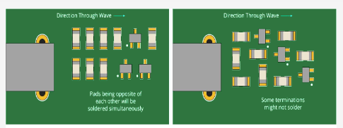
Step 2: Placement Strategies
- Critical components first:
- Place connectors according to mechanical design
- Position large ICs and heat-generating components
- Place clock generators and sensitive analog components
- Supporting components:
- Place decoupling capacitors close to IC power pins
- Group related passive components together
- Consider assembly and soldering requirements
- Use the “Auto-placement” tool cautiously:
- Often requires significant manual adjustment
- Can be helpful for initial placement of non-critical components
Part 4: Routing the PCB
Step 1: Manual Routing
- Select the “Track Mode” tool
- Choose appropriate layer (Top or Bottom)
- Click to start routing from a pad, click again to place vertices
- Use “Ctrl+Click” to switch layers (automatically inserts vias)
- Routing tips:
- Keep high-speed signals short and direct
- Avoid sharp angles (use 45° angles instead of 90°)
- Maintain consistent trace widths where possible
Step 2: Power and Ground Routing
- Use wider traces for power nets (1mm or more depending on current)
- Consider using power planes for complex designs
- Implement star grounding for analog circuits
- Ensure low-impedance return paths for high-frequency signals
Step 3: Autorouting (Optional)
Proteus offers an autorouter, but manual routing is often preferred:
- Configure autorouter settings (“Tools” > “Auto Router”)
- Set routing strategies and priorities
- Run autorouter (“Tools” > “Auto Router” > “Begin”)
- Carefully review and manually adjust results
Step 4: Design Rule Checking (DRC)
- Click “Tools” > “Design Rule Check”
- Review and correct any violations:
- Clearance errors
- Unrouted nets
- Copper pour issues
- Run DRC periodically during routing to catch issues early
Part 5: Final Touches
Step 1: Copper Pour (Ground Planes)
- Select “Zone Mode” tool
- Choose “Copper Pour” option
- Select appropriate net (typically GND)
- Draw area for copper pour
- Configure pour settings (clearance, thermal reliefs)
- Right-click and select “Pour All”
Step 2: Silkscreen and Documentation
- Add component designators:
- Use “Tag Mode” tool to adjust reference designator positions
- Ensure text is readable and doesn’t overlap pads/vias
- Add informative text:
- Use “2D Graphics Text” tool
- Include version numbers, copyright information, warnings
- Consider assembly markings:
- Pin 1 indicators
- Orientation markers
- Test points
Step 3: 3D Visualization
- Click “Output” > “3D Visualization”
- Inspect your board in 3D to:
- Check component clearances
- Verify mechanical fit
- Visualize final product appearance
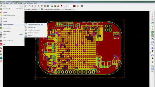
Part 6: Generating Manufacturing Outputs
Step 1: Gerber File Generation
- Click “Output” > “Gerber/Excellon Output”
- Select layers to include:
- Top Copper
- Bottom Copper
- Top Silk
- Top Solder Mask
- Bottom Solder Mask
- Board Outline
- Choose output directory
- Click “OK” to generate files
Step 2: Drill Files
- In the Gerber/Excellon dialog, ensure drill files are selected
- Configure drill file options (units, format)
- Verify drill file matches your board requirements
Step 3: Bill of Materials (BOM)
- In ISIS, click “Tools” > “Bill of Materials”
- Configure BOM format and content
- Generate report for procurement and assembly
Step 4: Assembly Drawings
- In ARES, click “Output” > “Assembly Drawings”
- Select appropriate views and layers
- Generate PDF or print directly
Best Practices for PCB Design in Proteus
- Schematic Organization:
- Use hierarchical design for complex circuits
- Group related components logically
- Clearly label all important nets
- Component Management:
- Verify footprints before placement
- Create custom components when needed
- Maintain a well-organized library
- Routing Techniques:
- Route critical signals first
- Minimize via usage in high-speed paths
- Maintain consistent impedance where required
- Design Verification:
- Run ERC and DRC at multiple stages
- Cross-probe between schematic and layout
- Use 3D visualization to catch mechanical issues
- Documentation:
- Keep thorough design notes
- Version control your designs
- Maintain complete manufacturing packages
Common Pitfalls and Troubleshooting
- Missing Connections:
- Verify all nets were transferred from schematic
- Check for unconnected pins or hidden power pins
- Footprint Mismatches:
- Double-check component dimensions
- Verify pin numbering matches schematic symbols
- Manufacturing Issues:
- Ensure adequate clearances for your fabricator’s capabilities
- Verify solder mask and silkscreen requirements
- Performance Problems:
- Review high-speed signal paths
- Check power distribution network
- Consider adding test points for debugging
Advanced Techniques
- Multi-layer Boards:
- Proper layer stacking for signal integrity
- Effective use of power and ground planes
- High-Speed Design:
- Impedance-controlled routing
- Length matching for differential pairs
- Proper termination techniques
- Flexible PCBs:
- Special layer configurations
- Bend radius considerations
- Embedded Components:
- Designing with components inside the PCB layers
- Special manufacturing requirements
Conclusion
Proteus provides a comprehensive environment for taking your electronic designs from concept to manufacturing-ready PCB layouts. By following this step-by-step guide, you can efficiently navigate through schematic capture, component placement, PCB routing, and final output generation.
Remember that PCB design is both an art and a science. While Proteus automates many aspects of the process, successful designs still require careful planning, attention to detail, and consideration of both electrical and mechanical requirements. As you gain experience with Proteus, you’ll develop your own workflow and design strategies that work best for your specific projects.
The key to mastering PCB design in Proteus is practice. Start with simple designs and gradually take on more complex projects as you become comfortable with the tools and techniques. Don’t hesitate to use Proteus’s extensive documentation and online resources when you encounter challenges.
With the skills you’ve learned in this guide, you’re now equipped to turn your electronic circuit ideas into professional-quality PCB layouts ready for manufacturing. Happy designing!