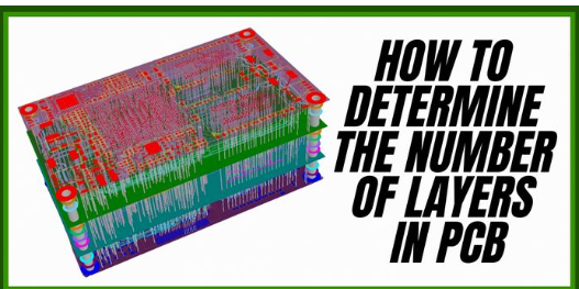
How to Identify the Number of Layers in a Motherboard PCB
Introduction
Printed Circuit Boards (PCBs) are the fundamental building blocks of all modern electronics, and motherboards represent some of the most complex PCB designs in common use. One critical aspect of motherboard quality and capability is its layer count—the number of conductive copper layers sandwiched between insulating material in the PCB stackup. Understanding how to determine a motherboard’s layer count is valuable for engineers, technicians, and even informed consumers who want to assess build quality, potential performance, and manufacturing sophistication.
This article provides comprehensive techniques for identifying the number of layers in a motherboard PCB through various inspection methods, from simple visual examination to more advanced analytical approaches.
Understanding PCB Layer Basics
Before attempting to identify layer count, it’s essential to understand what PCB layers are and why they matter:
- Signal layers: Carry electrical signals between components
- Power planes: Distribute power evenly across the board
- Ground planes: Provide shielding and stable reference voltages
- Mixed layers: Combine power, ground, and signal routing
Motherboards typically range from 4-layer designs in budget models to 12-layer or more in high-end platforms. More layers allow for:
- Better signal integrity
- Reduced electromagnetic interference (EMI)
- More complex routing possibilities
- Improved power delivery
- Enhanced thermal management
Method 1: Visual Inspection Techniques
1. Edge Examination
The most straightforward approach is examining the PCB edge where the layers are visible in cross-section:
- Hold the motherboard at an angle to light
- Look closely at the board’s edges, preferably with magnification
- Count the distinct dark lines (copper layers) separated by lighter substrate
Tips:
- Clean the edge if obscured by solder mask or contamination
- Use a bright light source at a low angle
- A jeweler’s loupe or microscope helps for precise counting
Limitations:
- Some manufacturers apply edge plating that obscures layers
- Very thin prepreg layers might be hard to distinguish
- Not all edges may reveal the complete stackup
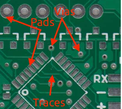
2. Via Inspection
Examine different types of vias (vertical interconnects):
- Through-hole vias: Go through all layers
- Blind vias: Connect outer layer to one or more inner layers
- Buried vias: Connect only inner layers
The presence of blind/buried vias typically indicates higher layer counts (6+ layers). Count visible via stubs on both sides of the board to estimate layers.
3. Component Density Observation
Higher layer counts often accompany:
- Densely packed components
- Fine-pitch BGAs (Ball Grid Arrays)
- Complex chipsets with many power phases
- Numerous small decoupling capacitors
While not definitive, dense layouts often require more layers for proper routing.
Method 2: Documentation Research
1. Manufacturer Specifications
Check:
- Product datasheets
- Technical white papers
- Marketing materials (often highlight layer count as a premium feature)
2. Board Silkscreen
Some motherboards print layer information:
- Near the model number
- Along the PCIe slots
- On reverse side near mounting holes
Look for notations like “8L PCB” or “6 Layer Design.”
3. Industry Databases
Resources like:
- PCB manufacturer reference designs
- Chipset vendor recommended layouts
- Teardown analyses from technical websites
Method 3: Physical Measurement and Calculation
1. Thickness Measurement
While not perfectly accurate, general correlations exist:
- Standard 1.6mm thickness: Typically 4-6 layers
- ~2.0mm: Often 6-8 layers
- >2.4mm: Usually 8+ layers
Measure with calipers at an unobstructed area.
2. Weight Comparison
More layers generally mean more weight:
- Compare with known layer count references
- Requires experience with different boards
Method 4: Advanced Techniques
1. X-ray Inspection
X-ray systems can:
- Visualize internal layers non-destructively
- Show layer-to-layer connections
- Reveal blind/buried via structures
2. Cross-Sectional Analysis
Destructive but definitive:
- Cut a small section of the board
- Polish the edge
- Examine under microscope
- Count visible copper layers
3. Time-Domain Reflectometry (TDR)
Advanced electrical method:
- Measures impedance discontinuities
- Can reveal layer transitions
- Requires specialized equipment
Method 5: Reverse Engineering Approaches
1. Schematic Analysis
For known designs:
- Trace critical signal paths
- Count necessary routing layers
- Add power/ground planes
2. Layer-by-Layer Delamination
(Note: Destructive method)
- Carefully sand or etch away outer layers
- Document each revealed layer
- Continue until all layers are exposed
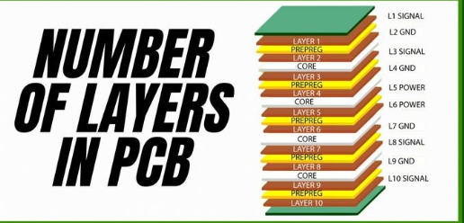
Common Motherboard Layer Configurations
Understanding typical stackups helps in identification:
4-Layer:
- Top Signal
- Ground plane
- Power plane
- Bottom Signal
6-Layer:
- Top Signal
- Ground
- Inner Signal
- Inner Signal
- Power
- Bottom Signal
8-Layer:
More complex arrangements with additional:
- Dedicated high-speed signal layers
- Split power planes
- Secondary ground planes
10+ Layer:
- Multiple specialized signal layers
- Several power domains
- Shielded high-speed channels
Practical Examples
Identifying a 4-Layer Board:
- Simple edge examination shows 4 distinct layers
- Limited component density
- Few or no blind/buried vias
- Typically 1.6mm thickness
Identifying an 8-Layer Board:
- Edge shows 8+ visible layers
- Complex BGA packages present
- Numerous blind vias visible
- Thickness around 2.0-2.4mm
- Often marketed as “high-end” or “premium”
Potential Pitfalls and Misidentifications
Common mistakes:
- Counting solder mask as a layer
- Missing very thin prepreg layers
- Confusing ground/pour with dedicated planes
- Overlooking that some layers may not reach board edges
Conclusion
Accurately determining a motherboard’s PCB layer count requires careful observation and often multiple verification methods. While visual edge examination provides a good starting point, combining techniques yields the most reliable results. Understanding layer count helps evaluate a motherboard’s design sophistication, potential signal integrity characteristics, and overall quality.
As motherboard designs continue evolving with increasing layer counts to support higher-speed interfaces and more complex power delivery systems, these identification skills remain valuable for engineers, technicians, and enthusiasts alike.
Remember that layer count is just one aspect of PCB quality—proper design and manufacturing execution are equally important. A well-designed 6-layer board may outperform a poorly implemented 8-layer design in actual use.