How to Improve PCB Routing Speed: Techniques and Best Practices
Introduction
Printed Circuit Board (PCB) design is a complex process that requires careful planning and execution. Among the various stages of PCB development, routing (or wiring) is often the most time-consuming aspect. As electronic devices become more sophisticated with higher component densities and more stringent performance requirements, the need for efficient PCB routing techniques has never been greater. This article explores practical strategies to significantly improve PCB routing speed without compromising design quality.
Understanding the Factors Affecting Routing Speed
Before diving into solutions, it’s essential to understand what makes PCB routing time-consuming:
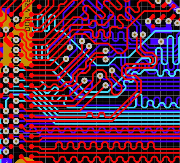
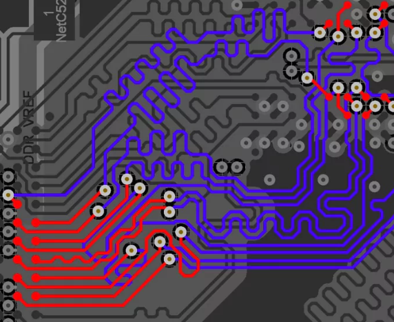
- Design Complexity: High-density interconnects (HDI), multi-layer boards, and high-speed signals increase routing difficulty
- Component Placement: Poor component placement can create routing bottlenecks
- Design Rules: Numerous constraints (clearances, impedance matching, etc.) slow down the routing process
- Tool Proficiency: Inadequate knowledge of the EDA (Electronic Design Automation) software features
- Revision Cycles: Frequent design changes require rerouting
Pre-Routing Preparation
1. Optimize Component Placement
“Good placement is half the routing done” – this adage holds true in PCB design. To facilitate faster routing:
- Group related components together based on their functional blocks
- Orient components to minimize crossing connections
- Place connectors and major components first
- Consider the routing channels during placement
- Use the “ratsnest” (connection lines) to identify potential placement issues
2. Establish Clear Design Rules Upfront
Configure all design rules before starting to route:
- Trace width and spacing requirements
- Via styles and limitations
- Layer stackup and usage definitions
- High-speed constraints (length matching, impedance control)
- Clearance rules for different voltage levels
Having these rules predefined allows the autorouter and interactive routing tools to work more efficiently.
3. Create a Logical Layer Stackup Strategy
Plan your layer usage carefully:
- Dedicate layers primarily to horizontal or vertical traces to minimize via usage
- Assign power and ground planes appropriately
- Consider microvia technology for HDI designs
- Use buried/blind vias when appropriate to reduce layer transitions
4. Develop a Routing Plan
Sketch a routing strategy:
- Identify critical signals that need special handling
- Plan the general flow of major busses
- Note areas that might require creative routing solutions
- Mark keep-out zones and restricted areas
Routing Techniques to Improve Speed
1. Master Interactive Routing Tools
Modern EDA tools offer powerful interactive routing features:
- Push-and-Shove: Lets you route through crowded areas by automatically pushing existing traces aside
- Auto-complete: Allows the tool to suggest complete connections based on your initial guidance
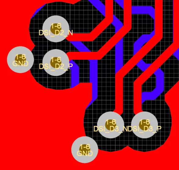
- Trace tuning: Quickly create serpentine patterns for length matching
- Differential pair routing: Specialized tools for routing balanced pairs
Invest time in learning these features through tutorials and practice.
2. Implement Efficient Autorouting Strategies
While pure autorouting often produces suboptimal results, strategic use can save time:
- Route critical signals manually first
- Use the autorouter for less critical connections
- Apply region-based autorouting for specific board areas
- Utilize bus routing features for parallel signals
- Run the autorouter in stages with different strategies
3. Leverage Routing Templates and Reuse
Create and use routing templates for:
- Common connection patterns (e.g., resistor arrays, decoupling capacitors)
- Frequently used bus structures
- Standard interfaces (USB, HDMI, etc.)
- Power distribution networks
Many EDA tools allow saving and reusing routing patterns across projects.
4. Utilize Advanced Routing Features
Explore these time-saving features in your EDA tool:
- Net classes: Apply routing rules to groups of nets
- Differential pairs: Define and route balanced pairs efficiently
- Length matching: Automatically tune trace lengths
- Interactive length tuning: Visually adjust trace lengths while maintaining topology
- Via shielding: Automatically place shielding vias along sensitive traces
5. Implement Hierarchical Design
For complex boards:
- Break the design into functional blocks
- Route blocks independently
- Connect blocks through carefully planned interfaces
- Use modular design approaches for reusable circuits
Post-Routing Optimization
1. Use Design Rule Checking (DRC) Effectively
- Run incremental DRC during routing to catch errors early
- Configure DRC to highlight only relevant violations
- Use batch DRC for final verification
2. Implement Smart Rerouting Techniques
When changes are necessary:
- Use “rip-up and retry” on specific segments rather than entire nets
- Employ “slide” features to adjust existing traces
- Utilize “retrace” functions that preserve basic routing topology
3. Automate Repetitive Tasks
Identify repetitive operations that can be automated:
- Script common routing patterns
- Create macros for frequent routing sequences
- Use batch processing for similar routing tasks
Tool-Specific Tips for Popular EDA Software
Altium Designer
- Use the ActiveRoute feature for semi-automated routing
- Leverage the Pin Swapping feature to reduce routing complexity
- Implement the xSignals technology for high-speed routing
Cadence Allegro
- Utilize the Auto-interactive Router (AIR)
- Implement the SKILL scripting for custom routing solutions
- Use the Constraint Manager extensively for efficient routing
Mentor Xpedition
- Apply the Sketch Router for quick routing concepts
- Use the Highway Router for bus routing
- Implement the AutoRouter in “guide” mode
KiCad
- Leverage the Push and Shove router
- Use the Differential Pair Router
- Implement custom track width rules for different net classes
Developing a Routing Mindset
Beyond technical skills, cultivate these habits:
- Think Ahead: Visualize the routing path before placing the first segment
- Work Methodically: Route in logical sequences (power first, then critical signals, etc.)
- Stay Organized: Use net classes, colors, and layers effectively
- Balance Perfectionism: Know when “good enough” routing suffices
- Continuous Learning: Regularly explore new routing techniques and tool features
Measuring and Tracking Routing Efficiency
To gauge improvement:
- Track time spent on routing versus other design phases
- Measure routing completion percentage over time
- Count manual interventions needed for autorouted sections
- Monitor error rates during DRC
Use these metrics to identify which techniques work best for your specific design scenarios.
Conclusion
Improving PCB routing speed is a multifaceted challenge that combines tool mastery, strategic planning, and efficient work habits. By implementing the techniques discussed—optimizing component placement, leveraging advanced EDA features, developing routing templates, and adopting a methodical approach—designers can significantly reduce routing time while maintaining or even improving design quality.
Remember that routing speed improves with experience. As you become more familiar with your EDA tools’ capabilities and develop your own routing strategies through practice, you’ll find yourself completing complex routing tasks in fractions of the time previously required. The key is to continuously learn, experiment with new approaches, and refine your process with each design iteration.
Ultimately, faster routing leads to shorter design cycles, allowing for more iterations and better optimization, which results in higher quality PCB designs delivered in less time—a competitive advantage in today’s fast-paced electronics industry.


