How to isolate the digital ground and analog ground of PCB
When designing a printed circuit board (PCB), the isolation of digital ground and analog ground is a very important link, because improper grounding will cause signal interference and increase noise, thus affecting the performance of the entire system.
1.Understanding digital ground and analog ground
Digital ground: usually refers to the reference ground of the digital circuit, which is used for the transmission and processing of digital signals.
Analog ground: usually refers to the reference ground of the analog circuit, which is used for the transmission and processing of analog signals.
2.The necessity of isolation
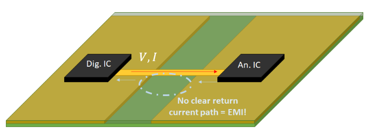
Digital signals and analog signals have great differences in frequency, amplitude and speed. If proper isolation is not performed, digital signals may introduce noise into the analog circuit through the ground line.
3.Isolation method
3.1 Physical isolation
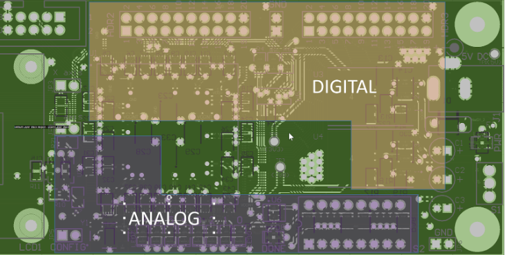
Ground plane division: In the PCB layout, the digital ground and analog ground are divided into two independent ground planes and connected through appropriate grounding points.
Ground line layout: Ensure that the digital ground line and the analog ground line do not cross to reduce mutual interference.
3.2 Electrical Isolation
Use isolation devices: such as optocouplers, magnetic couplers, etc., to transmit signals without directly connecting digital ground and analog ground.
Power supply isolation: Provide independent power supplies for digital and analog circuits, and power them through isolation transformers or DC-DC converters.
3.3 Grounding Technology
Single-point grounding: All ground wires are connected at one point to reduce noise caused by ground loops.
Multi-point grounding: Connect digital ground and analog ground at multiple points to reduce ground impedance and noise.
3.4 Shielding and filtering
Shielding: Use metal shielding covers or shielded cables to reduce external electromagnetic interference.
Filtering: Use filters between digital and analog circuits to reduce the transmission of high-frequency noise.

4.Design Practice
Layout optimization: Digital circuits and analog circuits should be laid out separately as much as possible to reduce mutual interference.
Wiring skills: Use wide and short ground wires to reduce ground impedance and noise.
Grounding point selection: Select grounding points reasonably to avoid forming ground loops.
5.Test and Verify
Ground Impedance Test: Measure the impedance between ground lines to ensure it is within the design range.
Signal Integrity Test: Check the quality of the signal to ensure there is no interference caused by ground line problems.